Global high-mix volume high-speed PCBA manufacturer
9:00 -18:00, Mon. - Fri. (GMT+8)
9:00 -12:00, Sat. (GMT+8)
(Except Chinese public holidays)
Global high-mix volume high-speed PCBA manufacturer
9:00 -18:00, Mon. - Fri. (GMT+8)
9:00 -12:00, Sat. (GMT+8)
(Except Chinese public holidays)
HomePage > Blog > Knowledge Base > PCB Wire Bonding: Materials, Techniques, Process, Applications and More
In today's rapidly developing electronic manufacturing industry, wire bonding plays an increasingly important role in the fields of PCB manufacturing and electronic packaging. Especially against the backdrop of the constantly rising demand for high-density and high reliability in electronic products, its importance has become increasingly prominent.
Compared with traditional bonding techniques, wire bonding can achieve a higher connection density and better electrical performance in a very small space. PCB wire bonding technology is one of the core processes for precisely interconnecting semiconductor chips and PCBs at the micrometer level. This technology is particularly applicable to the packaging applications of fine-pitch, high-frequency, high-power and thermally sensitive components.
Today, we will discuss the topic of PCB wire bonding. We will delve into the fundamental principles of PCB wire bonding, including material selection, bonding types, process flows, key application areas, and the best design practices. First of all, let's have a brief understanding of wire bonding.
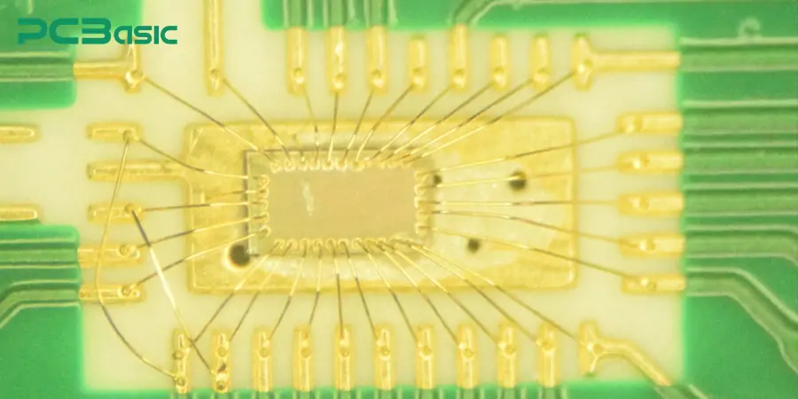
Wire bonding is a kind of microelectronic packaging technology. It electrically connects integrated circuits or semiconductor chips with their corresponding PCB bonding pads through fine metal wires (i.e., bonding wires). These wires are the key channels for signal transmission inside modern electronic devices.
Scenarios:
High-density fine-pitch interconnection is required
Thermal stress must be reduced
High-frequency or high-power devices have strict requirements for electrical and thermal performance
The chip needs to be directly installed onto the PCB to achieve compact packaging
In all the above scenarios, PCB wire bonding is very important. Because of the unique technological advantages of PCB wire bonding:
In compact packages where chips need to be directly installed on the PCB, wire bonding can provide a flexible connection method with high space utilization and low package height.
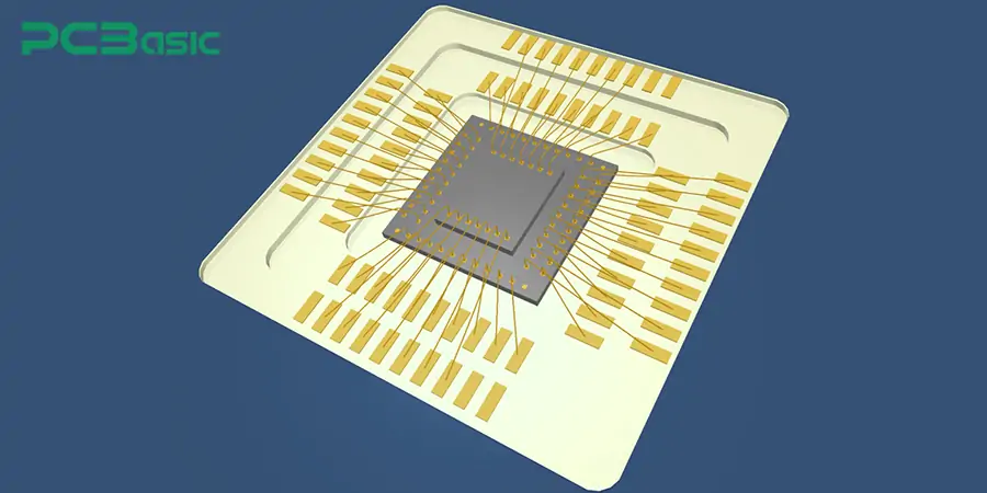
To meet the diverse requirements for reliability, performance and packaging processes in different application scenarios, the selection of materials used in PCB wire bonding is particularly crucial. What materials are there for PCB wire bonding? Next, we will introduce it in two parts: bonding wire materials and substrate and pad materials.
In PCB wire bonding, the main component connecting the chip and the circuit board is the bonding wire. Different types of wires have their own advantages and disadvantages, and are suitable for different application scenarios. The commonly used bonding wire materials are:
Gold Wire Bonding (Au)
Gold wire bonding has excellent corrosion resistance, high stability, outstanding bonding performance and a long service life. It is widely used in the fields of high-reliability wire bonding services such as aerospace, military industry and medical electronics. Although the cost of gold wire bonding is relatively high, its performance is excellent. It is very necessary for scenarios with high stability requirements.
Copper Wire Bonding (Cu)
Copper wire has excellent electrical conductivity, a cost much lower than that of gold, and high mechanical strength. It is widely used in consumer electronics, power modules, automotive electronics and other fields, and is currently one of the fastest-growing PCB wire bonding materials.
Aluminum Wire Bonding (Al)
Aluminum wire has strong oxidation resistance and is convenient for large-diameter bonding, making it highly suitable for high-current carrying. Moreover, aluminum wires are usually used in conjunction with ultrasonic wedge bonding technology. The bonding process requires lower temperatures, making it highly suitable for heat-sensitive components.
Palladium-Coated Copper wire (PCC)
Palladium-clad copper wire combines the excellent electrical conductivity of copper with the corrosion resistance of palladium. It is widely applied in semiconductor wire bonding, where extremely high long-term stability requirements are imposed. It belongs to high-end wire bonding materials and is suitable for applications in high-frequency, high-temperature and multi-climate environments.
Silver Wire
Silver has extremely strong electrical conductivity and good thermal conductivity. It is often used in special applications such as chip bonding or flip chip bonding, such as the packaging of certain sensors or high-frequency devices. However, due to cost and easy oxidation issues, it is used relatively less.
|
Material |
Advantages |
Applications |
Limitations |
|
Gold (Au) |
Corrosion resistant, stable |
Aerospace, military, medical |
Expensive |
|
Copper (Cu) |
Excellent conductivity, low cost |
Consumer, automotive, power |
Oxidation risk |
|
Aluminum (Al) |
Oxidation resistant, large wires |
High-current, heat-sensitive |
Lower conductivity |
|
PCC |
Conductivity + corrosion resistance |
Semiconductor, high-frequency |
Higher cost |
|
Silver (Ag) |
Best conductivity & thermal |
Sensors, flip chip |
Cost, oxidation |
Good bonding wires must be matched with appropriate PCB substrate and pad surface materials to ensure reliable wire bonding. Common substrate and pad surface materials include:
FR4 substrate
Fr4 substrate is the most commonly used rigid PCB material. Low cost and mature technology make it a common choice in standard PCB wire bonding. It can be said that the vast majority of electronic products will adopt this kind of substrate.
Ceramic substrates (AlN, Al₂O₃)
Ceramic substrates have high thermal conductivity, excellent insulation performance and good dimensional stability. It is often used for semiconductor wire bonding, especially in applications with high frequency, high power and high heat dissipation requirements, where the effect is outstanding.
Metal core PCB
The metal substrate has an extremely strong heat dissipation capacity and is suitable for the application of the wire bonding process of high-power chips. It is often used in power electronics, LED lighting modules and other occasions.
|
Substrate Material |
Key Features |
Applications |
|
FR4 |
Low cost, mature, widely used |
Standard PCB wire bonding, most consumer electronics |
|
Ceramic (AlN, Al₂O₃) |
High thermal conductivity, excellent insulation, stable |
Semiconductor wire bonding, high-frequency, high-power, high-heat |
|
Metal Core PCB (MCPCB) |
Excellent heat dissipation |
Power electronics, LED lighting, high-power chip bonding |
Surface Finishes
In order to ensure that the bonded wire can be soldered firmly, PCB pad surfaces must be properly treated, including ENIG, ENEPIG, and OSP. Good surface treatment can enhance the firmness of the weld and avoid issues such as weak bonding and bond failure. It is the basis for ensuring the reliability of wire bonding on the PCB.
The selection of materials is only the first step to ensure the reliability of soldering. To achieve high-quality connections, it is also necessary to adopt appropriate wire bonding techniques according to the specific packaging type, product application and process requirements. Next, we will introduce several main types of bonding techniques in PCB wire bonding.
1. Thermosonic Wire Bonding
Thermosonic wire bonding is currently the most widely used process in PCB wire bonding, especially in semiconductor packaging and advanced PCB assembly. This technology combines heating, ultrasonic vibration and pressure to firmly weld the "Bonding Wire" to the pad. However, a precise "Wire Bonding Machine" needs to be equipped to precisely control the temperature and ultrasonic power. It is commonly used in gold wire bonding and copper wire bonding, which is increasingly widely applied.
2. Ultrasonic Wedge Bonding
Ultrasonic wedge bonding uses ultrasonic vibration combined with appropriate pressure to complete the bonding at room temperature or low temperature. It is particularly suitable for the bonding of soft metals such as aluminum and is also very suitable for the "Wire Bonding on PCB" scenario where heat-sensitive components are located.
3. Ball Bonding (Gold/copper ball bonding)
Ball bonding is one of the most common wire bonding processes in high-density and fine-pitch applications. This process is widely used in gold wire bonding and the rapidly developing copper wire bonding. It can also achieve precise chip bonding and is highly suitable for the layout of small and highly integrated PCBs.
4. Hybrid Wire Bonding and Flip Chip Bonding
In some advanced PCB assemblies, manufacturers combine "Flip Chip Bonding" with "Wire Bonding", which can achieve the highest interconnection density and the optimal performance balance. This flexible process combination enables manufacturers to balance the three core requirements of performance, size and cost in both semiconductor wire bonding and PCB wire bonding applications. This hybrid technology is widely applied in multi-chip modules (MCM), system-in-package (SiP), and high-end radio frequency modules.
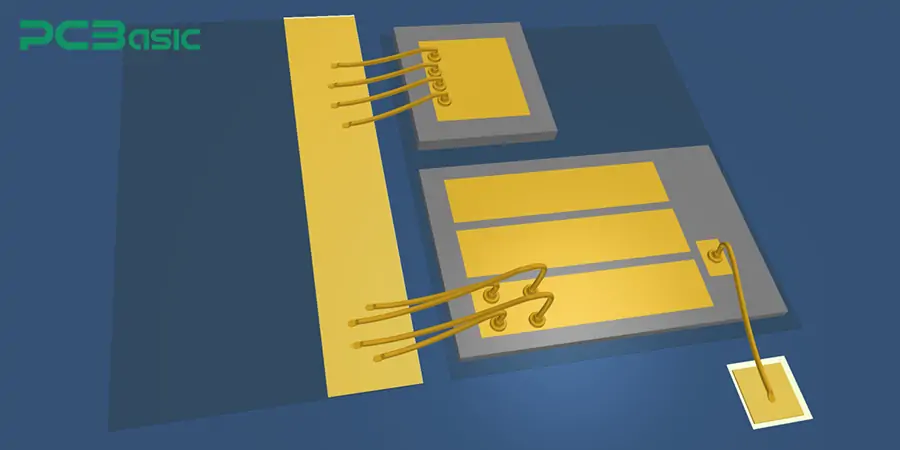
In the process of PCB wire bonding, each step will directly affect the soldering quality and long-term reliability. The following are the complete standard process steps of wire bond:
1. Substrate preparation and cleaning
Before starting the application of wire bonding on PCB, the PCB substrate needs to be thoroughly cleaned. The purpose of this step is to remove dust, oil stains, oxides and particles to avoid contaminants affecting the adhesion effect of the bonding wire. This step is the first line of defense to ensure reliable PCB bonding.
2. Chip mounting
If chip bonding is involved, the bare chips need to be fixed to the predetermined positions on the PCB or packaging substrate through adhesives or solders.
3. Wire selection and setting
According to the design requirements and application environment, we select the appropriate bonding wire materials, such as gold wire bonding or copper wire bonding. Meanwhile, we need to set the parameters of the wire bonding machine, such as wire diameter, tension and wire supply rate.
4. Calibration of capillary tools
Before the formal welding, the operator needs to calibrate the height, pressure and ultrasonic parameters of the capillary tool of the wire bonder. This step is to ensure the uniformity of the wire welding process and the welding strength.
5. Forming the first solder joint
In the thermosonic wire bonding or ball bonding processes, tiny welding balls are usually formed at the ends of the bonding wires first. The bonding ball or wedge-shaped end is bonded to the first pad through heat, pressure and ultrasonic vibration to form a strong metal bond.
6. Arc Forming and Control
After welding, the machine controls the bonding line to be pulled out at a specific Angle (Looping) to absorb the stress caused by subsequent thermal expansion and mechanical vibration. A good arc design is crucial for enhancing the long-term reliability of wire soldering on PCBs.
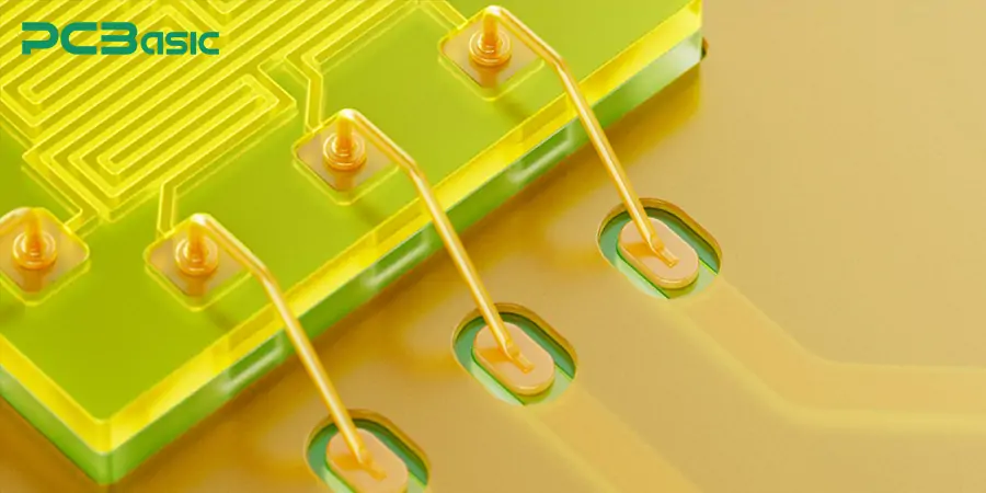
7. Forming the second solder joint
Fix the other end of the bonding wire to the corresponding pad or pin to complete the connection of the entire wire. The second solder joint is usually completed by wedge welding or ball tail welding techniques.
8. Tail line cutting and termination
When a section of wire is completed, the wire welding machine automatically cuts off the tail wire to prepare for the next circuit. The shearing action should be rapid and precise to avoid breaking the weld points or causing stress concentration.
9. Post-weld cleaning
To remove possible residual welding by-products or contaminants, necessary cleaning is required. This helps to improve the insulation and long-term stability of the final Bonded Wire.
10. Encapsulation or three-proof coating (optional)
In many high-reliability applications, after the PCB wire soldering is completed, packaging treatment is still required. If protected by potting compound, epoxy resin or conformal coating, it can prevent external moisture, dust or chemical corrosion from causing damage to the solder joints.
The application of PCB wire bonding is very extensive. In the following table, taking several common scenarios as examples, we list the common bonding methods, the main PCB wire materials and the challenges in production.
|
Application |
Key Features |
Common Bonding Methods |
Main Materials |
Challenges |
|
High-Frequency RF Modules & Antennas |
High-speed signals, low parasitics |
Thermosonic, Ball Bonding |
Gold, Copper |
Precise wire length, pad layout, minimize interference |
|
Power Modules (IGBT, MOSFET) |
High current & voltage, heat |
Ultrasonic Wedge, Aluminum Bonding |
Aluminum, Copper |
Thick wires, pressure control, avoid breakage |
|
Automotive & EV BMS |
Long life, vibration resistant |
Thermosonic, Copper, PCC Bonding |
Copper, PCC |
Handle thermal cycling, fatigue, humidity |
|
LED Arrays & Lighting |
Power dissipation, optical stability |
Ultrasonic Wedge, Thermosonic |
Aluminum, Copper |
Thermal control, heat dissipation, avoid wire shift |
|
Aerospace, Military & Satellite |
Extreme temps, radiation |
Thermosonic, High-Reliability Ball |
High-purity Gold |
Military standards, long-term stability |
|
Medical Implants & Sensors |
Biocompatibility, safety |
Thermosonic, Ball Bonding |
Gold |
Hermetic sealing, insulation integrity |
Wire bonding remains an irreplaceable core technology in modern PCB assembly. It features high precision, flexible design and superior performance, and is still widely used in various fields. By rationally selecting the bonding wire materials, matching the suitable PCB substrate and pad materials, and adopting the appropriate wire bonding process, we can achieve highly reliable, fine-pitch and high-performance electrical connections in multiple fields.
Whether in semiconductor wire bonding, flip chip bonding, or the traditional application of wire bonding on PCB, this technology has demonstrated extremely strong adaptability.
 About PCBasic
Time is money in your projects – and PCBasic gets it. PCBasic is a PCB assembly company that delivers fast, flawless results every time. Our comprehensive PCB assembly services include expert engineering support at every step, ensuring top quality in every board. As a leading PCB assembly manufacturer, we provide a one-stop solution that streamlines your supply chain. Partner with our advanced PCB prototype factory for quick turnarounds and superior results you can trust.
Assembly Enquiry
Instant Quote
Phone contact

+86-755-27218592
In addition, we've prepared a Help Center. We recommend checking it before reaching out, as your question and its answer may already be clearly explained there.
Wechat Support

In addition, we've prepared a Help Center. We recommend checking it before reaching out, as your question and its answer may already be clearly explained there.
WhatsApp Support

In addition, we've prepared a Help Center. We recommend checking it before reaching out, as your question and its answer may already be clearly explained there.