Global high-mix volume high-speed PCBA manufacturer
9:00 -18:00, Mon. - Fri. (GMT+8)
9:00 -12:00, Sat. (GMT+8)
(Except Chinese public holidays)
Global high-mix volume high-speed PCBA manufacturer
9:00 -18:00, Mon. - Fri. (GMT+8)
9:00 -12:00, Sat. (GMT+8)
(Except Chinese public holidays)
HomePage > Blog > Knowledge Base > Ultimate Guide to PCB Layout: Design, Tools, Guidelines, and Best Practices
Among electronic products today, whether it is smartphones, automotive electronics, wearable devices or satellite systems, one of the core components is the circuit board. It not only carries various electronic components but also is responsible for connecting and transmitting electrical signals. The foundation of all this is a reasonably planned PCB layout. An excellent PCB layout design will directly affect the performance, stability, heat dissipation effect and production efficiency of the product.
In product development, the success of a project often depends on reliable PCB design and layout. It not only involves circuit layout and component positions but also includes routing traces, setting up board layers, planning power delivery, simulation tests and manufacturing file preparation. Whether you are an engineer, a product manager, or an electronics enthusiast, it is very important to master the basic knowledge of PCB layout.
This article will take you to understand what PCB layout is, how to choose the appropriate PCB layout software, and how to do a good job in circuit board layout and follow the correct PCB layout guidelines so as to design a PCB board layout with excellent performance, high reliability and easy production.
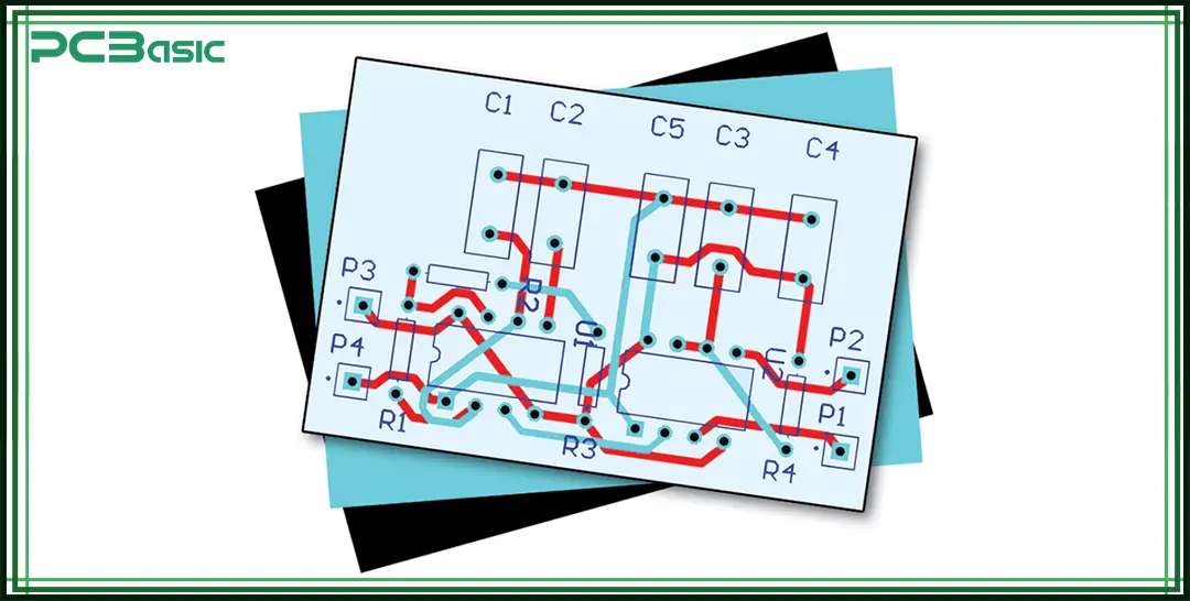
PCB layout refers to the physical design process of the printed circuit board (PCB). This step mainly involves placing electronic components in the right positions and connecting them with copper traces (conductive paths). The purpose is to transform the logical circuit design in the schematic diagram into a real and manufacturable circuit board layout.
It should be noted that PCB design and PCB layout are not the same thing. PCB design encompasses the entire process, such as drawing schematic diagrams, conducting circuit simulations, and preparing production files. The PCB layout is only a part of it, focusing on the board layout, that is, how the components are arranged, how the traces are routed, and how each layer is structured.
So, what is PCB layout? Simply speaking, it is the key step to turning ideas into physical products. It's the blueprint that transforms a concept into a working PCB board layout.
A standard PCB board layout usually includes the following important parts:
Substrate: This is the base material of the circuit board. The most common type is FR-4 (fiberglass). It provides structural support for the entire board and determines its strength and insulation performance.
Copper traces: Also known as wiring or routing, these are the conductive paths on the board. They connect the electronic components, transmitting electrical signals or power. They are the core of the circuit layout.
Pads and vias: Pads are metal points used for soldering components. Vias are used to conduct current between different layers, which is especially important in multilayer boards.
Components: These include various electronic devices such as resistors, capacitors, chips (ICs), and connectors. Each component serves a specific function, such as signal processing, power control, or communication.
Silkscreen layer: This is the layer printed on the PCB surface to show component labels, reference positions, company logos, or version information. It helps with assembly and maintenance.
When conducting PCB layout design, it is necessary to ensure that these elements are reasonably arranged on the circuit board. There should be sufficient spacing between components to prevent short circuits or interference. The traces should maintain electrical integrity to avoid signal loss or distortion. At the same time, thermal management should also be considered to ensure that heat can be effectively dissipated and prevent the device from overheating.
Only by planning all these factors well can an efficient PCB board layout that is both reliable and easy to manufacture be achieved.
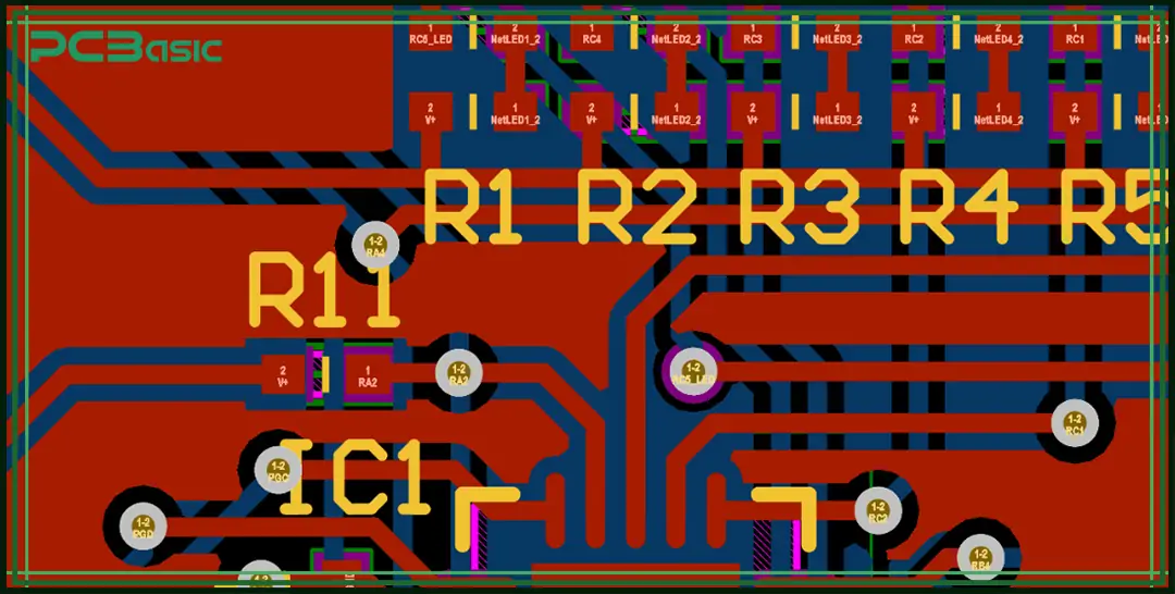
When conducting circuit board layout, choosing which type of layout is very crucial. This depends on the functional complexity of the product, its size, and the environment in which it is used. Different types of PCB layouts have significant differences in structure, cost, performance and manufacturability.
The following are several common types of circuit board layouts:
• Single-sided layout: All components and traces are placed on one side of the PCB. This PCB layout is simple and low-cost, ideal for basic products like toys, remote controls, and household electronics. However, space is limited, and the routing density is low, so it’s not suitable for high-performance devices.
• Double-sided layout: Components and traces can be placed on both sides of the PCB, which gives more flexibility in routing. It’s commonly used in medium-complexity electronics such as meters and industrial control boards. Compared to single-sided boards, the cost is slightly higher, but the functionality is better.
• Multilayer PCB layout: Usually refers to PCBs with 4 or more layers. These boards have power layers, ground layers, and signal layers stacked together, allowing for higher routing density and better electromagnetic compatibility. This type of PCB layout design is widely used in advanced equipment like communication devices, computer motherboards, and medical electronics.
• Rigid PCB layout: Uses a solid material like FR-4 as the base. It has a stable structure and is easy to manufacture. This is the most common type of PCB layout and fits most general-purpose electronic products.
• Flexible circuit layout: Uses flexible materials like polyimide as the base. It can bend and fold, making it ideal for tight spaces or moving parts, such as wearables, camera modules, and medical catheters.
• Rigid-flex board layout: Combines rigid and flexible boards into one. It allows 3D installation in compact areas and supports complex structural designs. This board layout is used in high-reliability applications such as aerospace, military devices, and foldable smartphones.
Overall, different types of PCB layouts not only affect the design approach and routing complexity but also directly relate to the cost, performance and long-term reliability of the product. Correctly choosing the layout type is the first step to achieving an efficient PCB board layout.
 About PCBasic
Time is money in your projects – and PCBasic gets it. PCBasic is a PCB assembly company that delivers fast, flawless results every time. Our comprehensive PCB assembly services include expert engineering support at every step, ensuring top quality in every board. As a leading PCB assembly manufacturer, we provide a one-stop solution that streamlines your supply chain. Partner with our advanced PCB prototype factory for quick turnarounds and superior results you can trust.
When conducting PCB layout design, it is very important to choose the appropriate PCB layout software. Good software can not only enhance work efficiency but also improve design accuracy, helping you complete the entire circuit board layout process faster and more reliably. Many advanced software also offer functions such as automatic routing, real-time Design Rule Check (DRC), and 3D modeling, which greatly simplify the design work of complex circuit boards.
At present, the commonly used PCB layout software mainly includes the following types:
• Altium Designer: Powerful and full of features. It’s made for big companies and is great for designing complex multilayer boards. It’s often used for high-end products.
• DipTrace: Easy to use and has a clean interface. It supports multilayer boards and 3D previews. Good for small to medium-sized projects.
• KiCad: Free and open-source. It has a strong user community and is always improving. Great for hobbyists, students, and startups.
• Eagle: Made by Autodesk. It’s affordable and fits well into the Autodesk design tools. Ideal for beginners and educational use.
• OrCAD: Very professional. It’s especially good for simulation and circuit design. Best for projects that need strong signal performance.

When choosing PCB layout software, there are some key features you should pay close attention to.
1. Schematic and Layout Integration
First, check if the software supports integration between schematics and layout. This means that when you draw a schematic, the software should be able to create a netlist and send it directly into your PCB layout design. This helps reduce mistakes and makes the design process faster.
2. Real-Time Design Rule Check (DRC)
Second, it’s important that the software supports real-time DRC (Design Rule Check). While you place parts or draw traces, the system should tell you right away if there’s a problem—like spacing too small, trace too thin, or via size not correct. This ensures your design is correct and ready for manufacturing.
3. High-Speed Signal Design Support
If you're working on high-speed circuits like communication devices or RF boards, the software should support high-speed signal design. It should help with things like differential pair routing, impedance control, and timing checks. These need special simulation tools.
4. 3D PCB Board Layout Preview
Besides 2D layout, today’s designs often need 3D checking. So, it's good if the software has a 3D PCB board layout preview. This helps you see if parts will collide, if the height is right, or if the board will fit in the case.
5. Manufacturing File Output (Gerber, BOM, etc.)
Finally, a good PCB layout software must be able to export full manufacturing files. This includes Gerber files, drill files, and BOMs (Bill of Materials). These files are needed to turn your design into a real product.
In short, using the right PCB layout software with the right tools can greatly improve your circuit layout work. It helps you work faster, make fewer mistakes, and finish your project on time.
A good PCB layout needs a clear and organized design process. By following each step carefully, you can create a PCB board layout that is reliable, works well, and is easy to manufacture.
Before you start the board layout, you need to finish the schematic. This means adding all the components, connecting them properly, giving each part a name or number, and setting the design rules. This step is the starting point of the whole PCB design and layout process.
Next, you set up the layers of the board. This includes deciding how many signal, ground, and power layers you need, what materials to use, and how thick each layer should be. You also need to set the overall size of the board. This step is important for building a solid PCB board layout.
Now, you can place the parts on the board. Put important parts like the CPU, power chips, and ports first. Try to keep all the parts facing the same way to make soldering and repair easier. Follow PCB layout guidelines so the parts are spaced well and don't interfere with each other. Group similar parts together to make routing easier later.
After placing the parts, it's time to draw the paths (traces) that connect them. For high-speed signals, keep the traces the same length to avoid timing problems. Make traces short and straight, and don't use sharp angles. Use copper pours for ground areas to make signals cleaner. Try not to use too many vias because they can weaken signal quality.
When routing is done, run a design rule check (DRC). This step helps you find problems like short circuits, wrong connections, or parts that are too close. It also makes sure your circuit board layout follows the rules for making a real board.
Following a clear PCB layout designing process helps you work faster, avoid mistakes, and create better-quality PCBs every time.
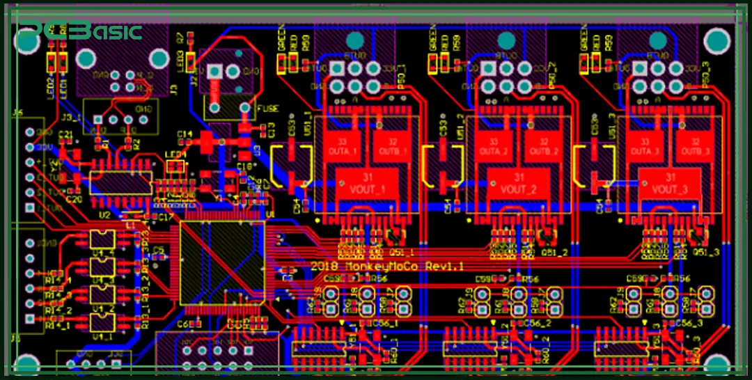
To get better performance and stability, follow these important PCB layout guidelines when designing your board:
1. Logical Component Placement
Put input and output parts on opposite sides of the board. Group parts that work together in the same area. This makes your PCB layout cleaner and helps reduce signal problems. It also makes routing easier.
2. Minimize Loop Area
For high-speed signals or big currents, keep the loop area small. A smaller loop helps stop signal noise and cuts down on electromagnetic radiation. This makes your system more stable.
3. Keep Analog and Digital Circuits Separate
Analog signals can be easily affected by noise. Keep analog parts away from digital parts. This helps protect signal quality and keeps your circuit board working correctly.
4. Avoid Right-Angle Traces
Try not to make 90-degree corners in your traces. Use 45-degree angles or curves instead. This helps stop signal reflections, which is important for fast signals.
5. Use Large Ground Planes
Cover as much of the board as possible with a ground plane. This gives signals a smooth path to return and blocks electromagnetic interference (EMI).
6. Add Decoupling Capacitors
Put decoupling capacitors close to the power pins. They remove power noise and help give chips clean power. This is an important step in PCB layout design.
7. Use Vias to Connect Ground Layers
Add extra vias to link different ground layers. This lowers resistance and improves the strength of the ground in your whole PCB.
8. Clear Silkscreen Markings
Label the silkscreen layer clearly. Show part numbers, directions, and version info. This helps with assembly, testing, and fixing later.
By following these PCB layout guidelines, you can avoid EMI, overheating, and logic errors. It also helps your circuit board last longer and work better.
A successful PCB layout is an important bridge between circuit design and physical products. Whether you are developing a simple LED module or a complex micro-control system, following the PCB layout design process and best practices of the system is an important guarantee for ensuring functionality, reliability and manufacturability.
Choosing the appropriate PCB layout software, following the design rules, placing components reasonably and optimizing the traces are the keys to high-quality PCB design and layout. With the advancement of technology, proficiency in PCB layout designing is no longer an additional skill but an essential ability for electronic engineers.
Q1: What is the difference between PCB design and PCB layout?
PCB design covers the entire process from schematic creation to final manufacturing, while PCB layout specifically refers to the component placement and routing stage, also known as the circuit board layout.
Q2: What software is best for PCB layout?
Popular PCB layout software includes Altium, KiCad, Eagle, DipTrace, and OrCAD. The best choice depends on your budget, experience level, and project complexity.
Q3: What are the key rules for circuit layout?
Basic PCB layout guidelines include proper trace spacing, functional area grouping, avoiding right-angle traces, maintaining good grounding, and checking signal integrity.
Q4: How can I make sure my PCB layout meets manufacturing requirements?
Use the DRC (Design Rule Check) features in your PCB layout software, follow IPC standards, communicate with your manufacturer early, and review Gerber and drill files before production.
Q5: Can I design a multilayer PCB without professional software?
While free tools like KiCad can handle basic PCB layouts, designing complex multilayer PCB board layouts is best done with professional software for better efficiency and accuracy.

Assembly Enquiry
Instant Quote
Phone contact

+86-755-27218592
In addition, we've prepared a Help Center. We recommend checking it before reaching out, as your question and its answer may already be clearly explained there.
Wechat Support

In addition, we've prepared a Help Center. We recommend checking it before reaching out, as your question and its answer may already be clearly explained there.
WhatsApp Support

In addition, we've prepared a Help Center. We recommend checking it before reaching out, as your question and its answer may already be clearly explained there.