Global high-mix volume high-speed PCBA manufacturer
9:00 -18:00, Mon. - Fri. (GMT+8)
9:00 -12:00, Sat. (GMT+8)
(Except Chinese public holidays)
Global high-mix volume high-speed PCBA manufacturer
9:00 -18:00, Mon. - Fri. (GMT+8)
9:00 -12:00, Sat. (GMT+8)
(Except Chinese public holidays)
A proper paneling method can enhance the production accuracy and assembly efficiency during PCB manufacturing and assembly. Therefore, we recommend that customers adopt a reasonable PCB paneling plan during the design stage. A good PCB paneling can simultaneously process multiple circuit boards in the same production batch. This not only reduces manual handling but also improves the consistency of SMT and THT mounting. At PCBasic, each PCB panel will first undergo professional automated and manufacturability verification.
Recommended standard PCB panel dimensions:
Minimum panel size: 50 × 50 mm
Maximum panel size: 330 × 530 mm
PCB panels within this range can be perfectly compatible with fully automatic SMT conveyors, high-speed surface mount equipment, AOI, and precision paneling machines. In addition, it helps maintain mechanical stability during assembly and prevents vibration and warping. The panel design can be provided by you. If you are unsure about the suitable PCB panel size, you can contact us. Our engineers will provide you with professional services.
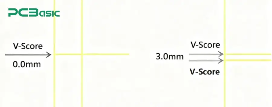
When using the v-scoring / v-cut / v-groove process for board separation, the v-shaped notches must run through the entire assembly board without interruption or deviation. The spacing between the circuit boards can be designed to be 0 millimeters or 3 millimeters.
A spacing of 0 millimeters is suitable for high-density, small composite boards. A spacing of 3 millimeters can enhance mechanical strength and reduce the stress risk during the board separation process. The specific choice depends on the assembly method and the requirements of the circuit board separation process.

If your assembly board contains multiple circuit boards of different sizes or shapes, PCBasic recommends that you use Tab Routing instead of V-cutting.
For the tab routing paneling method, regardless of whether there are breakouts (stamp holes), a reasonable pitch and the structure of the tabs are very important. When using this paneling method, the distance between the panels should be 1.6 mm. This not only leaves sufficient space for the milling cutter but also ensures the overall mechanical support strength of the paneling.
① Tab route with breaking holes (stamp holes)
Breakthrough hole diameter: ≥ 0.45 mm (typically 0.55–0.6 mm)
Pore spacing: ≥ 0.35 mm
We usually need to design 5-6 slots to ensure adequate board separation strength. This type of panel assembly design is one of the most common forms of panel assembly currently.
② Tab route with tab (no holes)
Eccentricity width: ≥ 2.0 mm
Solid tab routing connects each sub-board through solid tabs, resulting in greater overall strength.
In some designs, both v-cut scoring and tab routing can be used simultaneously. In such cases, the following points should be noted:

The spacing between the plates in the V-shaped area should be 3 mm.
The spacing between the boards in the rat-run panel area should be 1.6 mm.
Note: In most automatic soldering (SMT) and assembly lines, edge rails need to be set up to facilitate the conveyance by the conveyor belt and the positioning of the fixtures. A 5–10 mm border should be added to each side.
Fiducial marks, tooling holes, barcodes or logos should be placed on the edge rails. After the board is separated, the borders can be easily removed.
Fiducial Marks

When assembling PCBs, fiducial marks are required. At least three reference marks should be set on each PCB board. We recommend a fiducial mark diameter of 1.0 millimeters and a solder mask opening diameter of 1.7 millimeters.
The fiducial marks should be placed in the central area of the panel border, which is more convenient for the visual system of the SMT assembly machine to recognize and automatically align. As shown in the figure below,
Mounting Holes
In addition to the fiducial marks, each panel should also be designed with 4 positioning holes for fixture installation, conveyor track positioning, and test fixture alignment. The diameter of the holes can be referred to the following diagram:

Lean more about PCB panel assembly here.
Assembly Enquiry
Instant Quote
Phone contact

+86-755-27218592
In addition, we've prepared a Help Center. We recommend checking it before reaching out, as your question and its answer may already be clearly explained there.
Wechat Support

In addition, we've prepared a Help Center. We recommend checking it before reaching out, as your question and its answer may already be clearly explained there.
WhatsApp Support

In addition, we've prepared a Help Center. We recommend checking it before reaching out, as your question and its answer may already be clearly explained there.