JS@pcbasic.com

Ru

Help Center  
Sending a message
Open Hours:9:00-21:00 (GMT+8)
Service hotlines
+86-755-27218592

Open Hours:9:00-21:00

(Except Chinese public holidays)

X

How to order pcb stencil in Pcbasic, your smt stencil manufacturer

The process of ordering pcb stencil in pcbasic is very simple. As an smt stencil maker, we have more advantages. We have a dedicated PCB Stencil Online Quote for you. You can tick each option according to your needs. Our pcb smt stencil MOQ is 1. As a pcb stencil maker, no matter how many stencil pcb assembly we can provide for you. When you fill in the quantity of pcb stencil you need, the system automatically calculates the price of the order, and you click Submit to complete the order. In addition, Pcbasic as one of the best SMT stencil manufacturers, We have prepared special offers for you.

1. If you have pcba order in pcbasic, we can give you a pcb stencil for free
2. If your PCB and components purchase amount reaches 10,000 US dollars, we will give you pcb stencil for free

Pcb Stencil Frame Type Stencil mesh Steel sheet
Pcb Stencil Polishing Process Grinding polish (no additional charge) Electrolytic polishing (with additional fee)
Pcb Stencil Production method Top layer Bottom Layer Top and Bottom (On Single Stencil) Top and Bottom Layer (On Separate Stencil)
Pcb Stencil Dimension(cm) 30* 40CM 30*40CM 37* 47CM 42* 52CM 45* 55CM 58.4*58.4CM 55* 65CM 73.6*73.6CM 40*60CM 40*70CM 40*80CM 40*100CM 40* 120CM 40* 140CM 50* 70CM 50*80CM 50* 120CM
Pcb Stencil thickness(mm) 0.08mm 0.10mm 0.12mm 0.15mm 0.2mm
Pcb Stencil Qty pcb stencil MOQ : 1
Pcb Stencil Type Solder paste mesh Red glue mesh
Pcb Stencil Fiducial Marks no Non Half-cut marks through hole Mark NPTH Hole
Pcb Stencil Engineering processing requirements According to the “Steel Mesh Production Specification and Agreement” for production you need to confirm the pdf file to cut
Pcb Stencil Billing Information No need invoice Need invoice
What Is A Pcb Stencil?

Stencils, also known as SMT stencils (SMT Stencil), are a special mold for SMT. Its main function is to aid in the deposition of solder paste; the purpose is to transfer the exact amount of solder paste to the exact location on the empty PCB. It started with nylon (polyester) mesh.

Later, there was barbed wire mesh, copper wire mesh, and finally stainless steel mesh due to durability. But no matter what material the wire mesh is, it has the disadvantages of poor molding and low precision. Affected by the cost of materials and the difficulty of production, the original steel mesh was made of iron/copper plate, but because it was easy to rust, stainless steel mesh replaced them, which is the current steel mesh (SMT Stencil).

Types Of Pcb Stencils

The production process of SMT steel mesh can be divided into:

  • laser template
  • electropolishing template
  • electroforming template
  • step template
  • bonding template
  • nickel plating template
  • etching template
1. Laser Stencil

Laser stencil formwork is currently the most commonly used formwork in the SMT stencil industry. Its characteristics are: Directly using data files for production, reducing production errors; SMT template opening position accuracy is very high: the whole process error ≤ ± 4μm; The opening of the SMT stencil has geometric figures, which is beneficial to the printing and forming of the solder paste. The following materials are required to make a laser stencil: A.PCB The PCB must be in the correct version, without deformation, damage, or breakage; B. Data file The data must contain the SMT solder paste layer (including Fiducial Mark data and PCB shape data), and must also contain character layer data, so as to check the front and back of the data, component types, etc.

2. Electropolishing Stencil (E.P.Stencil)

The electropolishing template is to post-process the steel sheet by the electrochemical method after laser cutting to improve the opening hole wall. Its characteristics are A. The whole wall is smooth, especially suitable for ultra-fine pitch QFP/BGA/CSP. B. Reduce the wiping times of the SMT template and greatly improve the work efficiency.

3. Electroforming Stencil (E.F.Stencil)

In order to meet the requirements of short, small, light, and thin electronic products, ultra-fine volume (such as 0201) and ultra-dense pitch (such as ūBGA, CSP) are widely used. In this way, the SMT stencil industry has also put forward more requirements for printing stencils. High requirements, electroforming template came into being. The characteristics of the electroforming template produced by our company are: Different thicknesses can be made on the same template.

4. Step Stencil

Due to the different requirements for the amount of solder paste when welding various components on the same PCB, the thickness of some areas of the same SMT template is required to be different, which results in the STEP-DOWN&STEP-UP process template. STEP-DOWN template Localized thinning of the stencil to reduce the amount of tin when soldering specific components.

5. Bonding Stencil

The COB device has been fixed on the PCB, but the patch process of tin printing is still required, which requires the use of a Bonding template. The bonding template is to add a small cover to the PCB bonding position corresponding to the template to avoid the COB device to achieve the purpose of flat printing.

6. Ni.P. Stencil

In order to reduce the friction between the solder paste and the hole wall, facilitate demolding, and further improve the release effect of the solder paste, at the beginning of 2004, Wei Chuangxin Company added a special post-processing method based on the traditional subtractive process “electropolishing” template. Treatment additive process – “nickel plating”, and patented. Nickel-plated stencils combine the advantages of laser stencils and electroforming stencils.

7. Etching Template Stencil

It is made of 301 type steel sheet imported from the United States. The etched steel mesh is suitable for PCB board printing with an angle and spacing greater than or equal to 0.4MM. It is suitable for copying boards and films. CAD/CAM and exposure methods can be used at the same time. For scaling, there is no need to calculate the price according to the number of parts. The production time is fast. The price is cheaper than the laser template. It is convenient for the customer’s film archive.

How To Make Pcb Stencil

The production process of steel mesh includes chemical etching, laser cutting, and electroformed.

1. Chemical etching

Process flow: data file PCB→film making→exposure→developing→etching→steel cleaning→opening Features: One-time molding, faster speed; cheap price. Disadvantages: It is easy to form an hourglass shape (insufficient etching) or the opening size becomes larger (over-etching); objective factors (experience, medicine, film) have a great influence, there are many production links, and the cumulative error is large, not suitable for the fine pitch stencil production method; The production process is polluting, which is not conducive to environmental protection.

2. Laser cutting

Process flow: film making PCB → taking coordinates → data file → data processing → laser cutting → grinding → Zhangwang Features: High precision of data production, the small influence of objective factors; trapezoidal opening is conducive to demoulding; precision cutting can be done; the price is moderate. Disadvantages: cut one by one, the production speed is slow.

3. Electroforming method (electroform)

Process flow: coating the photosensitive film on the substrate → exposure → development → electroforming nickel → forming → steel sheet cleaning → netting Features: The hole wall is smooth, especially suitable for the ultra-fine pitch stencil manufacturing method. Disadvantages: The process is difficult to control, the production process is polluted, which is not conducive to environmental protection; the production cycle is long and the price is too high.

PCB Stencil Service Opening Design

1. Three factors of the opening pcb stencil design

The opening design of the stencil should consider the release property of the solder paste, which is determined by three factors:

Among the three factors, the latter two are determined by the manufacturing technology of the steel mesh, and we consider the former more. Because the laser stencil is very cost-effective, the China pcb stencil focus on the opening design of the laser stencil.

First, we know the aspect ratio and area ratio:

Generally speaking, to obtain a good demoulding effect, the width-thickness ratio should be greater than 1.5, and the area ratio should be greater than 0.66. When should the aspect ratio be considered and when should the area ratio be considered? Generally, if the length of the opening does not reach 5 times the width, the area ratio should be considered to predict the release of the solder paste, and the aspect ratio should be considered in other cases.

2. Electropolishing Stencil (E.P.Stencil)
Component Type PITCH Pad width Pad length Opening width Opening length Template thickness Width and thickness ratio Area ratio
QFP 0.635mm 0.35mm 1.45mm 0.30-0.31mm 1.45mm 0.15-0.18mm 1.7-2.1 0.69-0.85
QFP 0.50mm 0.254mm 1.25mm 0.22-0.24mm 1.20mm 0.12-0.15mm 1.5-2.0 0.62-0.83
QFP 0.43mm 0.20mm 1.25mm 0.19-0.20mm 1.20mm 0.10-0.12mm 1.6-2.0 0.68-0.85
QFP 0.30mm 0.18mm 1.00mm 0.15mm 0.95mm 0.07-0.10mm 1.5-2.1 0.65-0.93
BGA ∮1.27mm ∮0. 8mm ∮0. 75mm 0.15-0.18mm 1.0-1.25
BGA ∮1.0mm ∮0.5mm ∮0. 48mm 0.12-0.15mm 0.80-1.0
uBGA ∮0.8mm ∮0.4mm ∮0. 40mm 0.12-0.15mm 0.67-0.83
uBGA ∮0.8mm ∮0.4mm □0. 38mm □0. 38mm 0.12-0.15mm 0.63-0.79
uBGA ∮0.5mm ∮0.25mm □0. 28mm □0. 28mm 0.08-0.10mm 0.70-0.86
0402 0.5mm 0.65mm 0.48mm 0.635mm 0.10-0.12mm 1.4-1.37
0201 0.25mm 0.40mm 0.235mm 0.38mm 0.08-0.10mm 0.73-0.91

Of course, when designing the opening of the steel mesh, the width-thickness ratio or the area ratio cannot be blindly pursued and other process problems, such as continuous tin, multi-tin, etc., are ignored. In addition, for chip components above 0603 (1608), we should think more about how to prevent tin beads.

3. opening design of the gluing process smt stencil (SMT template):

Because of its characteristics, the experience value of opening design is very important. The opening of the rubber stencil is generally opened into a long strip or a round hole; two positioning holes should be opened when the non-MARK point is positioned. Remarks:

4. SMT Stencil (SMT template) opening design tips:

Post-processing of PCB Stencil

Etching and electroforming stencils generally do not do post-processing, and the post-processing of stencils mentioned here is mainly for laser stencils. Because metal slag will adhere to the walls and openings after laser cutting, surface grinding is generally required; of course, grinding is not only to remove the slag (burr) but also to roughen the surface of the steel sheet. Increase the surface friction to facilitate the rolling of the solder paste and achieve a good effect of tin removal. If necessary, “electropolishing” can also be selected to improve the hole wall for complete slag removal (burr).

How to use pcb stencils

SMT steel mesh is a “squeamish” precision mold, therefore, you should pay attention to:

Factors affecting the quality of pcb stencils

There are mainly the following factors that will affect the quality of the steel mesh:

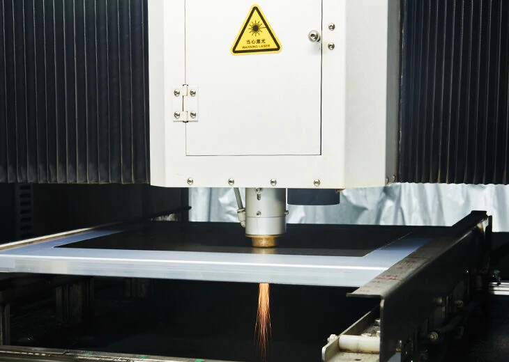
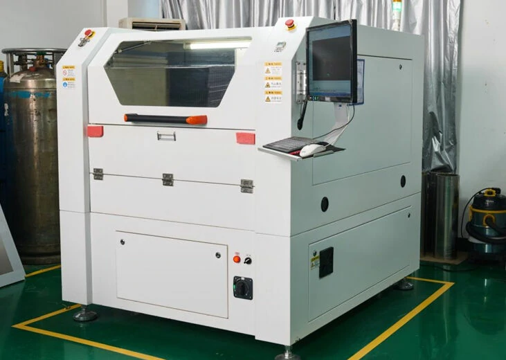
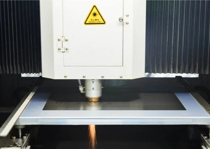
1.Production process of stencil pcb assembly

We have discussed the production process of steel mesh earlier. We can know that the best process should be electro-polishing after laser cutting. Both chemical etching and electroforming have processes that are prone to errors such as longevity film, exposure, and development, and electroforming is also affected by the unevenness of the substrate.

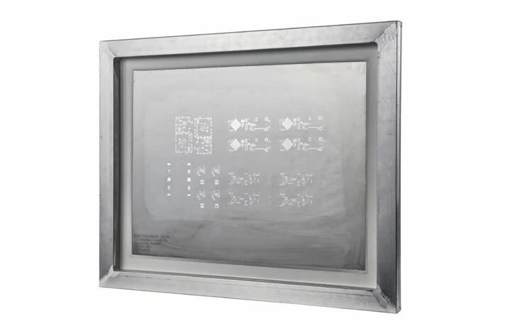
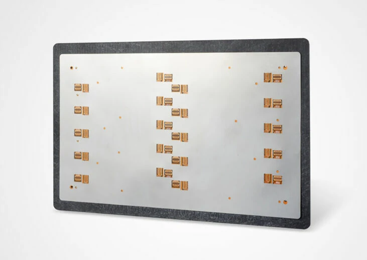
2. Stencil pcb assembly Materials used

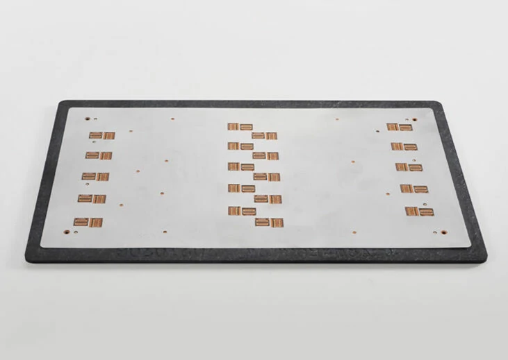
Including frame, wire mesh, steel sheet, adhesive, and so on. The screen frame must be able to withstand a certain program of relay and have a good level; the wire mesh is best to use polyester mesh, which can keep the tension stable for a long time; the best steel sheet is No. 304, and the matt one is better than the mirror one. It is more conducive to the rolling of solder paste (glue); the adhesive must be strong enough and resistant to certain corrosion.

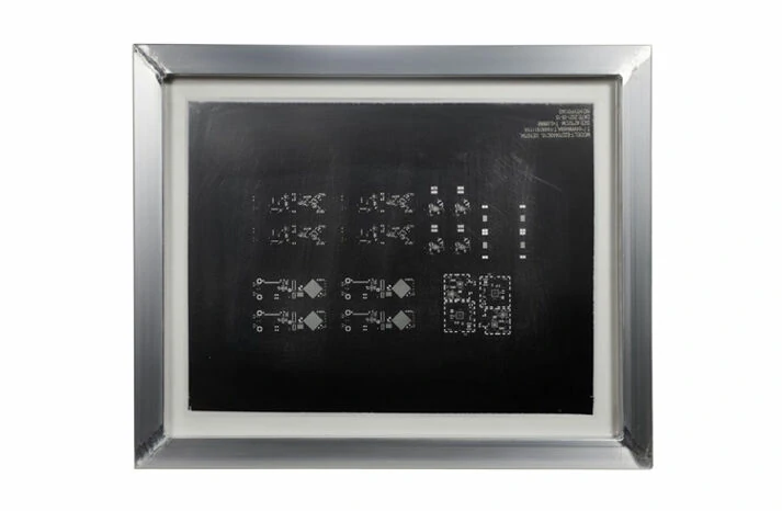
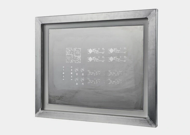
3. Stencil pcb assembly Opening design

The quality of the opening design has the greatest impact on the quality of the steel mesh. As discussed above, the design of the opening should take into account the manufacturing process, width-to-thickness ratio, area ratio, experience value, etc.

4. Pstencil pcb assembly information

The integrity of the production materials will also affect the quality of the steel mesh. The more complete the data, the better. At the same time, when the data coexist, it should be clear which one shall prevail. Also, generally making stencils from data files minimizes errors.

5. How to use smt stencil

The correct printing method can keep the quality of the stencil. On the contrary, incorrect printing methods such as excessive pressure, uneven stencil or PCB during printing, etc., will damage the stencil.

6. Cleaning for smt stencil

Solder paste (glue) is relatively easy to cure. If it is not cleaned in time, the opening of the stencil will be blocked, and the next printing will be difficult. Therefore, after the stencil is removed from the machine or the solder paste is not printed on the printing machine for 1 hour, it should be cleaned in time.

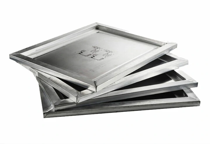
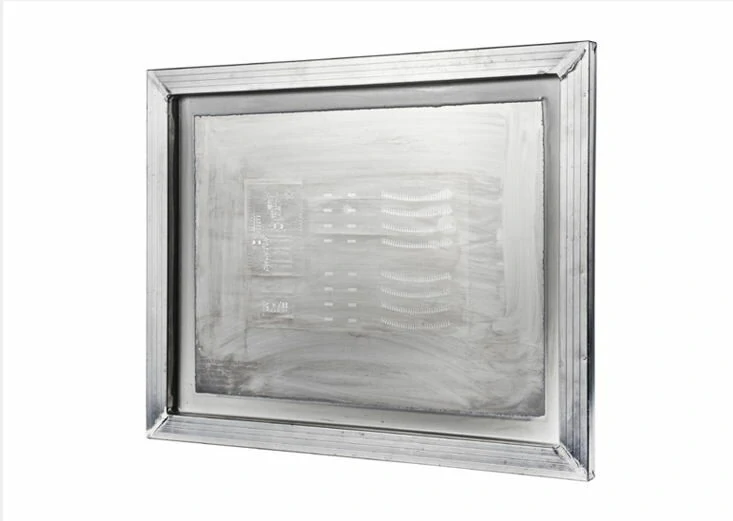
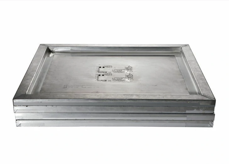
7. Storage for smt stencil

The stencil should be stored in a specific storage place and should not be placed randomly, so as to avoid accidental damage to the stencil. At the same time, the steel mesh should not be stacked together, so that it is not easy to handle and may bend the mesh frame.

Factors affecting the quality of pcb stencils

SMT stencils must be cleaned before, during, and after use (usually cleaned with SMT stencil cleaning machines):

1. Stencil cleaning methods
① wipe

Wipe the stencil with a lint-free cloth (or special stencil wiper) pre-soaked with the cleaner to remove cured solder paste or glue. It is characterized by convenience, no time limit, and low cost; The disadvantage is that it can not completely clean the stencil, especially the fine pitch stencil. In addition, some printing machines have an automatic wipe function, which can be set to automatically wipe the bottom of the stencil after printing several times. This process also uses a special steel mesh to wipe the paper, and the machine will spray the cleaning agent on the paper before the action.

② Ultrasonic cleaning

There are mainly two types of ultrasonic cleaning: immersion and spray, and some manufacturers use a semi-automatic ultrasonic cleaning machine to clean the steel mesh.

2. Choice of cleaning agent

The ideal stencil cleaner must be practical, effective, and safe for people and the environment, and it must also be able to remove solder paste (glue) from the stencil well. There are special stencil cleaners now, but it may wash out the stencil, so be careful when using them. If there is no special requirement, alcohol or deionized water can be used instead of the special cleaner for stencils.

To make the industry more efficient, come to PCBasic for free sample assembly.

PCBasic firmly believes that quality is the soul of products, and strictly abides by every standard, every process of production, and every detail of service!

Quote
E-mail