HDI PCBs | Design Basics and
Manufacturing Process
Miniaturization changed everything. More
layers. Finer traces. Tighter spacing. But standard PCBs can’t keep up.
Enter HDI—High Density Interconnect.
These boards use microvias, thin dielectrics, and advanced lamination to route
complex signals in compact footprints. You’ll find them in smartphones, RF
modules, medical implants, and advanced driver-assistance systems. It’s not
just smaller—it’s smarter routing, better signal integrity, and higher
reliability.
In this guide, we'll break down HDI PCB
and microvia structures and explain why this tech drives modern
high-performance electronics.
What Is an HDI PCB?
HDI stands for High Density Interconnect.
But it’s more than just a compact circuit board. It’s an advanced design
strategy used to squeeze more functionality into less space—without sacrificing
performance. These boards use microvias, blind and buried vias, ultra-thin
dielectrics, and multiple stacked layers to achieve incredibly dense routing.
You won’t find these in basic consumer
gadgets. A high density interconnect PCB is critical in high-performance
systems—think aerospace controls, 5G modules, LiDAR systems, neural implants,
and military-grade communications. Anywhere size, speed, and reliability
matter, HDI shows up.
They’re designed to handle fine-pitch
components, often under 0.5 mm. That allows tighter connections, faster
signals, and reduced electromagnetic interference. Traditional PCBs simply
can’t support that level of complexity.
It’s not just about saving space. HDI PCB
technology reduces signal loss, improves power delivery, and supports faster
switching speeds. In a world driven by AI, edge computing, and compact sensor
systems, HDI has become essential infrastructure—quietly powering the next wave
of intelligent electronics from the inside out.
Structure of HDI PCBs
Now, let’s talk about what makes an HDI
board different under the hood. Traditional PCBs have large mechanical drilled
vias and relatively wide traces. HDI PCBs use:
• laser-drilled
microvias,
• tighter trace
spacing,
• and stacked layer technology.
The entire structure is designed to
optimize every square millimeter. There’s a clear reason for that: the demand
for more I/O, smaller components, and higher speed signals.
Layer Structure
Common HDI PCBs follow a 1+N+1 structure,
where:
• "N" is the
number of core layers.
• The “1” on either side are the outer HDI layers connected by microvias.
It doesn’t stop there. Advanced HDI
layouts use 2+N+2. It has:
• Two HDI layers on
the top and two on the bottom.
• More routing channels. More room to breathe.
Still not enough? You can push it
further: 3+N+3, or even higher. It’s a scalable approach. You only add layers
when the design actually needs them, which keeps costs (and headaches) under
control.
Any-layer HDI, also called ELIC (Every
Layer Interconnect), removes the limits. Microvias can now connect any two
layers directly—no need to go step-by-step. Routing becomes insanely efficient.
This is how your smartphone gets all that performance packed into a board
smaller than a credit card.
These boards are built using sequential
lamination. That means you laminate, drill, plate, and repeat the process layer
by layer. This allows ultra-precise connections between dense internal
circuitry.
The structure usually includes:
• Core layer: Usually FR-4 or a
high-performance laminate.
• Prepreg: Resin-impregnated
fiberglass sheets that bond copper layers.
• Copper foil: For signal traces
and planes.
• Microvias: Laser-drilled holes less than 150 microns in diameter, plated with
copper.
All these elements come together to
support BGAs (Ball Grid Arrays) with 0.4mm pitch or smaller. That’s nearly
impossible with traditional via technology.
One key point: HDI isn’t just about
shrinking things. It’s about enabling reliable performance in compact layouts.
That requires perfect layer registration, consistent via plating, and precise
alignment during fabrication.
HDI PCB Stack-Up
Designers often say: if you get the
stack-up wrong, the board will fail—no matter how good your layout is.
An HDI PCB stack-up is more than just an
arrangement of copper and dielectric layers. It’s a carefully engineered
electrical architecture. Every layer serves a function—signal, power, ground, shielding—and
the via strategy ties it all together.
Let’s walk through a simplified HDI
stack-up:
1. Top Signal Layer
2. Dielectric
(Prepreg)
3. Ground Plane
4. Core
5. Power Plane
6. Dielectric
7. Bottom Signal Layer
Sounds straightforward, right? Not
exactly. In HDI design, microvias and blind/buried vias create vertical
connections between specific layers. You may have a via from Layer 1 to Layer
2, and a separate buried via from Layer 3 to Layer 5. Or a stacked via that goes
from Layer 1 all the way to Layer 6.
These choices aren’t random. They’re
based on:
• Signal timing
requirements
• Impedance control
• Crosstalk
minimization
• Power distribution and decoupling strategies
For high-speed digital designs—say, DDR4,
USB 3.0, or HDMI—you’ll often see dedicated stripline or microstrip
impedance-controlled traces embedded in specific layers. And all of this is
packed into a board that might only be 0.8mm thick.
Advanced HDI PCB stack-ups can include:
• Multiple buried via
layers
• Resin-coated copper
foils
• Filled and capped
via-in-pad structures
• Hybrid materials for specific electrical or thermal properties
One real-world example: a mobile
processor PCB might use a 3+N+3 stack-up, with 10 total layers, stacked
microvias, and resin-filled via-in-pad to support a 0.35mm BGA pitch.
Key takeaway? In HDI PCBs, the stack-up
is a performance tool—not just a mechanical one. It determines signal
integrity, EMI behavior, and even manufacturability.
Lamination & Materials for HDI
Boards
At this point, it's clear HDI design is
only half the battle. Manufacturing is the other. HDI boards are built through
sequential lamination cycles. That means layers are pressed, drilled, plated,
and bonded one at a time. Each lamination adds new routing options via
microvias and buried vias. But materials matter just as much as process.
Common Materials in HDI PCBs:
• FR-4 (High Tg variants): Cheap
and reliable for moderate-speed designs.
• Polyimide: Great thermal
stability for aerospace and defense.
• Rogers, Isola, Panasonic Megtron:
Used in high-speed RF/microwave HDI applications.
• Halogen-free or Lead-free
laminates: Meet strict environmental standards.
What Makes Materials
HDI-Compatible?
• High glass
transition temperature (Tg)
• Low Z-axis expansion
• Tight Dk/Df
tolerances for signal integrity
• Stable dielectric properties over frequency and temperature
Laser drilling also requires materials
with clean ablation behavior, so the edges of microvias remain intact without
debris or undercutting. Resin systems need to flow properly during lamination
but cure with high rigidity.
In short, your choice of material isn't
just about cost. It directly affects drillability, reliability, and RF
performance.
Key Benefits of HDI PCBs
Here’s what sets it apart:
1. Compact Size
HDI PCBs pack more routing density into
less board area. That’s critical when designing for devices like wearables,
implantables, or edge-AI modules. There’s no space for oversized traces or
full-depth vias. Microvias and fine-line routing let you scale down without
cutting features. No dead zones. No wasted space. Just an efficient layout.
2. Improved Signal Integrity
Shorter signal paths. Fewer stubs. Better
controlled impedance. Microvias reduce inductance, which leads to cleaner
high-speed signal transmission. That’s a big deal when you're routing DDR,
PCIe, USB 3.2, or HDMI signals.
3. Layer Count Optimization
Need a 12-layer board? With HDI, you
might get it done in 8 layers. That’s lower material cost, reduced board
thickness, and simpler lamination. Stacked microvias help in efficient layer
usage, so the layout stays compact and efficient.
4. Reduced Crosstalk & EMI
Smaller vias = tighter coupling. That
means reduced loop areas and less radiated noise. HDI is ideal when
electromagnetic compatibility (EMC) becomes critical—like in medical, avionics,
or automotive applications.
5. Thermal and Power Management
Microvia-in-pad designs improve thermal
dissipation. Also, more routing space allows better decoupling capacitor
placement, which directly enhances power delivery.
6. Mechanical Strength
Less drilling. No large through-holes.
Better copper balance. HDI boards offer more robustness under vibration and
thermal cycling—an important consideration in defense, aerospace, and EVs.
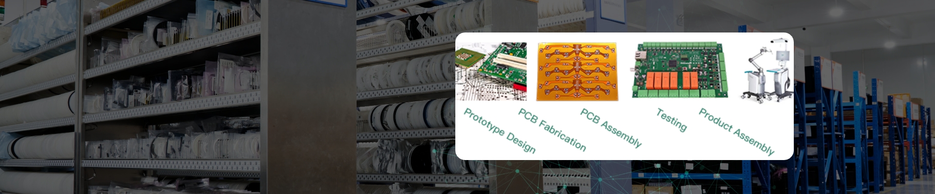
About PCBasic
Time is money in your projects – and PCBasic gets it. PCBasic is a PCB assembly company that delivers fast, flawless results every time. Our comprehensive PCB assembly services include expert engineering support at every step, ensuring top quality in every board. As a leading PCB assembly manufacturer, we provide a one-stop solution that streamlines your supply chain. Partner with our advanced PCB prototype factory for quick turnarounds and superior results you can trust.
Common Usages of HDI PCBs
HDI technology isn't limited to consumer
electronics. It's everywhere. Here's where HDI shows up behind the scenes:
1. Smartphones and Tablets
Space is the enemy. HDI PCBs help squeeze
CPUs, RAM, cameras, and batteries into sleek enclosures—without performance
compromise. Most modern smartphones have ELIC HDI boards with 10+ layers.
2. Medical Devices
Implantable defibrillators. Wearable
glucose monitors. Portable ECG. These products require ultra-small form factors
and strict reliability. HDI makes them possible.
3. Automotive Electronics
ADAS, infotainment, LiDAR control boards,
and electric vehicle battery management systems all benefit from HDI layout.
Especially with increasing autonomous functions, signal integrity and
miniaturization are non-negotiable.
4. Networking Equipment
Routers, switches, and base stations need
HDI boards for high-speed data routing, precise impedance control, and reduced
EMI.
5. Military and Aerospace
Defense-grade radar modules, avionics
processors, and navigation controls rely on HDI’s durability and signal clarity
in extreme environments.
HDI PCB Design Guidelines
Designing an HDI board is part science,
part art. You're not just placing traces. You're managing
physics—electromagnetic behavior, thermal expansion, and manufacturability
constraints. That's why the HDI layout demands special attention.
Here’s what matters most in HDI PCB
design.
1. Via Selection Strategy
• Microvias: Use them to connect
two adjacent layers. Avoid stacking more than 3 levels unless necessary.
• Staggered vs Stacked: Staggered
microvias are more reliable, but stacked allows tighter BGA escape.
• Buried Vias: Keep them isolated to inner layers. Plan their locations early to
avoid routing issues.
2. Via-in-Pad Design
Used in dense BGA packages, especially
when pitch goes below 0.5mm. These vias must be filled, plated, and planarized
properly to avoid solder wicking.
Not every fabricator can do this well.
Always consult with your HDI PCB manufacturer before committing.
3. Trace and Space Rules
• Trace width: Often between 3–4
mil for HDI.
• Spacing: Keep signal trace
spacing ≥2× trace width if possible to reduce crosstalk.
• For controlled impedance, simulate your stack-up using field solvers or
tools like Polar Si9000.
4. Aspect Ratio Considerations
Microvias have low aspect ratios—less
than 1:1. That’s why the depth between layers matters.
Avoid placing too many microvias in one
area. It can cause resin voids or uneven copper plating.
5. Via Fill and Reliability
Filled and capped vias are essential for
stacked structures. Use resin-filled or electroplated fill based on IPC
standards.
Incomplete via fill = reliability issues
= failed board in the field.
6. DFM and DFA Checks
Before tape-out, run checks for:
• Drill registration
• Solder mask
alignment
• Copper-to-copper
clearances
• Thermal reliefs
• Via tenting or capping
The goal? Fabrication-ready design with
minimal revisions.
HDI PCB Manufacturing Process
Manufacturing HDI boards is nothing like
regular PCBs. It’s multi-step, precision-driven, and highly sequential.
Here’s a simplified flow:
1. Inner Layer Imaging & Etching: Inner
copper layers are patterned using photolithography.
2. Core Lamination: The etched cores are laminated with prepreg and copper foil.
3. Laser Drilling
(Microvias): Laser drills sub-0.15mm vias through the
top layer. UV or CO2 lasers are typically used.
4. Desmearing and Hole
Cleaning: Plasma cleaning ensures debris-free via
holes for reliable plating.
5. Electroless Copper
Deposition: A thin copper layer is deposited inside
microvias for conductivity.
6. Electroplating: Additional copper is plated to increase via wall thickness.
7. Outer Layer Imaging &
Etching: Top signal layers are created. Fine traces
are patterned.
8. Sequential Lamination: Additional layers are added as needed, repeating steps 3–7 for each
HDI cycle.
9. Via Fill &
Planarization: Via-in-pad structures are filled with
epoxy resin and planarized via CNC.
10. Solder Mask and Surface Finish: ENIG or OSP surface finishes are applied.
11. Final Testing: Finally, electrical tests validate integrity.
This process may include multiple lam
cycles depending on stack-up complexity. Each cycle introduces cost and time,
so it must be engineered wisely.
Types of Vias in HDI Routing
In HDI boards, vias aren’t just holes.
They’re design elements.
Here’s a quick breakdown:
Through-Hole Vias
Go from top to bottom. Not used often in
HDI due to space wastage.
Blind Vias
Connect the outer layer to an internal
layer. Great for surface-mount component routing.
Buried Vias
Stay completely within inner layers.
Useful for keeping outer layers clean.
Microvias
Laser-drilled, <150µm diameter.
Connect adjacent layers. Low inductance and perfect for HDI.
Stacked Microvias
Placed directly on top of one another.
Enable vertical connection from top to core.
Staggered Microvias
Offset by a small amount. More
mechanically reliable than stacked.
Via-in-Pad
Placing via directly beneath a pad. Used
for ultra-dense BGAs and helps reduce inductive delay.
Each type has trade-offs in terms of
cost, manufacturability, and signal performance. Your choice should align with
the layout, stack-up, and component pitch.
PCBasic: Your Reliable HDI PCB
Manufacturer in China
Design is only half the equation. The
hard part? Turning that design into a board that actually works—down to the
micron.
That’s where PCBasic delivers.
We don’t just make PCBs. We build
HDI—from tight-pitch prototypes to full production runs. Need a 1+N+1? We’ve
got it covered. Running 3+N+3 or ELIC? No problem.
Why engineers choose PCBasic:
• Laser drilling
precision to 75 µm
• Controlled impedance
tuning
• Microvia reliability
testing
• IPC 6012, ISO, and
RoHS compliance
• Custom stack-up
engineering
• Quick-turn HDI PCB
prototyping
• DFM consultation included
We’ve helped clients across medical,
aerospace, telecom, and automotive industries. Whether you need a small HDI PCB
prototype or full volume production, we’re equipped to deliver.
Have a project in mind? Let’s talk.
Conclusion
HDI PCBs are essential today. They’re no
longer just a choice—they’re the standard. When your design needs more space,
faster speeds, or better signal integrity, HDI is the answer. From structure to
stack-up, understanding the details is crucial for success.
Whether you're a startup or an
established team, the right design and manufacturer matter. Precision is
everything.
Looking for a reliable HDI PCB partner?
Choose PCBasic because we know the tech and deliver quality every time.
We use cookies to enhance your experience, analyze traffic, and provide personalized content. By clicking “Accept Cookies”, you agree to our Cookie and Privacy Policy.
Manage Cookie Preferences
We use cookies to enhance your browsing experience. Please review the details of each cookie category below and choose your preferences.
Strictly Necessary Cookies
These cookies are essential for the website to function properly and cannot be disabled. They are typically set in response to actions you take, such as logging in or adding items to your shopping cart.
Performance Cookies
These cookies help us understand how visitors interact with our website by collecting information about traffic and usage. This allows us to measure and improve the website’s performance.
Targeting/Advertising Cookies
These cookies are used to deliver
advertisements relevant to you and your interests. They may also limit the number of times you see an
advertisement and help measure the effectiveness of advertising campaigns.
In addition, we've prepared a Help Center.
We recommend checking it before reaching out, as your question and its
answer may already be clearly explained there.
✖
Wechat Support
In addition, we've prepared a Help Center.
We recommend checking it before reaching out, as your question and its
answer may already be clearly explained there.
✖
WhatsApp Support
In addition, we've prepared a Help Center.
We recommend checking it before reaching out, as your question and its
answer may already be clearly explained there.


 About PCBasic


