Global high-mix volume high-speed PCBA manufacturer
9:00 -18:00, Mon. - Fri. (GMT+8)
9:00 -12:00, Sat. (GMT+8)
(Except Chinese public holidays)
Global high-mix volume high-speed PCBA manufacturer
9:00 -18:00, Mon. - Fri. (GMT+8)
9:00 -12:00, Sat. (GMT+8)
(Except Chinese public holidays)
HomePage > Blog > Knowledge Base > Common Types of Soldering Defects in Electronics Manufacturing
Soldering is a crucial process in electronic manufacturing, which firmly combines various independent electronic components with a bare printed circuit board (PCB) to form a functional electronic component that can work properly. Without reliable soldering, the circuit cannot conduct normally, and the product cannot perform as it should.
However, even in modern electronics factories equipped with advanced automated production equipment, soldering defects can still occur. These defects not only weaken the long-term reliability of electronic products but may also cause the equipment to malfunction in the early stage of use or even be scrapped directly. At the same time, the appearance of soldering defects will force manufacturers to rework or scrap products, thereby increasing production costs and prolonging delivery cycles.
Therefore, for manufacturers, understanding various types of soldering defects is key to ensuring product quality. Mastering the appearance, causes, and inspection methods of different soldering defects can not only help quickly identify bad soldering examples, but also effectively avoid common solder joint defects. Make sure that the solder joints of each PCB are stable and firm.
This article will systematically introduce the most common types of soldering defects, analyze their causes one by one, and provide easy-to-implement detection and prevention strategies in combination with production practice, which can help you solve various soldering defects easily.

Soldering defects refer to various imperfect, abnormal or non-compliant conditions that occur at solder joints or soldering areas when electronic components are connected to circuit boards using solder. These problems may be caused by operator errors, poor process control, contaminated material, poor equipment condition, or unsuitable environmental conditions such as temperature and humidity.
Why must we pay attention to various types of soldering defects? Because each type of defect not only has a different appearance, but also has its own unique causes, detection difficulty and impact on product performance, and therefore corresponding solutions are also different.
Common causes include:
• Solder Joint Formation Defects: such as insufficient solder, solder bridges, solder ball defects, etc.
• Component Placement & Process-Related Defects: such as component shift, tombstoning, skipped solder, etc.
• Material & Contamination-Related Defects: such as blowholes, contamination residues, shadowing effect, etc.
• Mechanical & Thermal Stress Defects: such as solder joint cracks, wire breakage, heat loss, etc.
During the soldering process, being able to identify these bad soldering examples and accurately analyze their causes is the first step to avoid the recurrence of similar solder joint defects, reduce expensive rework costs and lower the failure rate of finished products.
In the soldering process of PCBs and components, different types of soldering defects can be classified according to their causes and appearance characteristics. To facilitate understanding and analysis, here we classify them into four major categories.
The most common type is solder joint formation defects. This type of problem occurs at the initial stage when solder joints are formed between component leads and PCB pads. Once it appears, it will directly affect the soldering quality and circuit reliability. Solder joint formation defects are usually caused by the following reasons:
1. Insufficient / Excess Solder
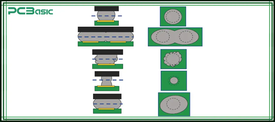
Insufficient solder is one of the most common soldering defects. When the amount of solder is too small, there may be gaps at the solder joints or the connection may not be firm, and both mechanical strength and electrical conductivity will be affected. Usually, incorrect stencil design, low solder paste volume or poor wetting will affect solder usage and soldering quality.
Excess solder, on the other hand, can lead to another type of problem, such as solder bridges (short circuits) or hindering the installation of adjacent components. Both of these cases are typical bad soldering examples, which not only affect the appearance but also reduce the mechanical and electrical properties of the product.
2. Solder Bridges
Solder bridge refers to the situation where excess solder forms a conductive connection between two adjacent pads, thereby causing a short circuit. This kind of solder joint defect is commonly seen in situations such as excessive solder paste printing, component misalignment, or uncontrolled solder flow during reflow soldering.
3. Cold Solder Joint
The characteristic of a cold solder joint is that the solder does not melt completely or cools too quickly, and the surface of the solder joint is dull and grainy. This is a very dangerous and common bad soldering example because it leads to poor conductivity, unstable contact, and solder joint failure in the early stage of product use.
4. Solder Balling
Solder ball defect refers to many tiny solder balls scattered on the surface of the PCB. This is usually caused by solder paste splashing during reflow soldering, insufficient flux activity or improper temperature profile control. Although these solder balls are unsightly in appearance, the greater risk is that they may cause short circuits after detachment.
5. Nonwetting / Dewetting
Nonwetting refers to the situation where the molten solder fails to bond with the surface of the pad or lead, while dewetting occurs when the solder initially wets and then retracts, resulting in the exposure of a metal surface. Both of these solder defects will seriously affect the electrical continuity and long-term reliability of the solder joints.
6. Gap in Solder Joint
The gaps inside the solder joints are usually caused by gas being trapped during the soldering process or poor solder flow. Such solder joint defects can reduce the strength of the solder joint, making it more prone to fracture when subjected to mechanical stress or thermal cycling.
7. Sunken Solder Joint
The surface of a sunken solder joint is concave, which is usually caused by insufficient solder or excessive heating time. This is also an obvious bad soldering example, because it not only affects the mechanical support of the solder joint, but may also cause the solder joint to be more prone to damage.

Time is money in your projects – and PCBasic gets it. PCBasic is a PCB assembly company that delivers fast, flawless results every time. Our comprehensive PCB assembly services include expert engineering support at every step, ensuring top quality in every board. As a leading PCB assembly manufacturer, we provide a one-stop solution that streamlines your supply chain. Partner with our advanced PCB prototype factory for quick turnarounds and superior results you can trust.
This type of soldering defect occurs during the mounting or soldering of components due to incorrect component positions, improper operation methods, or inadequate control of the soldering process. These defects not only affect the appearance of the solder joints but also directly impact the stability of the electrical connection and the long-term reliability of the product.
1. Component Shift
During the reflow soldering stage, if components move during high-temperature heating, the leads and pads will be misaligned, making it hard to form a correct solder joint.
2. Tombstoning
This phenomenon refers to the situation where one end of the chip component is lifted up, like a standing tombstone, while the other end remains soldered onto the PCB. This kind of bad soldering example often occurs during reflow soldering, mostly due to uneven heating or different wetting rates of the pads at both ends.
3. Skipped Solder
When there is no solder covering a pad or component lead at all, skipped solder occurs, resulting in an open circuit in the electrical circuit.
4. Lifted Pad
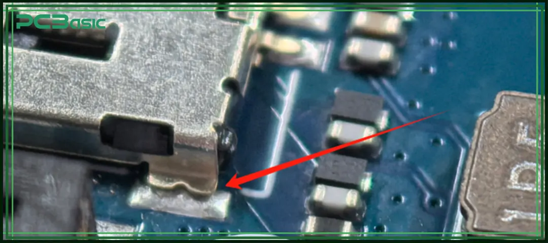
If the temperature is too high during soldering or excessive mechanical stress is applied during desoldering and rework, it may cause the copper pads to peel away from the PCB substrate. This is a serious solder joint defect, which is difficult to repair and usually requires replacement or extensive rework.
5. Surface Mount Defect
Such defects include component placement misalignment, reverse orientation installation, or failure to closely adhere to the PCB surface during SMT mounting.

During the soldering process, the quality of the material and the cleanliness of the production process have a very significant impact on preventing various types of soldering defects. Even if the soldering process parameters are properly controlled, if the material itself has problems or is not cleaned well, serious quality risks may still arise.
1. Blowhole/Pinhole
The so-called porosity or pinhole refers to the tiny voids that appear inside the solder joint. This is usually caused by the gas inside the solder joint not escaping smoothly during the solidification process of the solder and getting trapped in the solder joint. This type of solder defect can significantly reduce the mechanical strength and structural stability of the solder joint, making it more prone to cracking due to vibration, shock or temperature changes during long-term use.
2. Contamination/Chemical Residue
After soldering is completed, if there are fluxes, cleaning solutions or other chemical substances remaining on or around the solder joint surface, these substances may corrode the metal surface and even cause leakage and short circuits in the circuit. Such bad soldering examples often occur when the cleaning process is inadequate or inferior flux is used.
3. Shadowing Effect
The shadowing effect refers to the situation during wave soldering where certain components, due to their positions or heights, block the flow of the soldering wave, preventing the solder from fully covering the blocked pads or leads, thus resulting in incomplete or cold solder joints.
Solder joint defects may also occur during the subsequent operation of the product, because solder joints may be repeatedly subjected to different forms of mechanical stress and thermal stress during use, and will be damaged over time.
1. Fractured Solder joint
This defect refers to the appearance of fine or even visible cracks inside the solder joint. The common cause is metal fatigue resulting from thermal cycling or continuous vibration.
2. Wire Breakage
When the leads or component pins are repeatedly bent during use or subjected to excessive mechanical shock, metal breakage is prone to occur at the solder joints. Since the solder joint is the most fragile connection between the wire and the PCB, this soldering defect often directly leads to circuit failure.
3. Heat Loss
During the soldering process, if the heat from the soldering area is rapidly carried away by the nearby large area of copper foil, metal casing or heat dissipation structure, it will cause insufficient temperature at the solder joint, preventing the solder from fully melting and wetting, and ultimately resulting in insufficient solder.

To ensure the high reliability of the product, manufacturers usually adopt multiple detection methods to detect and evaluate various types of soldering defects. These methods include both manual inspection and automated and precision instrument detection, each with its own scope of application and advantages.
|
Inspection Method |
Description |
Detection Scope |
Advantages |
|
Visual Inspection (Manual Inspection) |
Trained inspectors examine solder joints using the naked eye or magnifying tools |
Solder bridges, cold solder joints, tombstoning, lifted pads, and missing components |
Low cost, immediate feedback |
|
Automated Optical Inspection (AOI) |
High-resolution cameras with image processing software compare actual assemblies to reference images |
Solder bridges, component misalignment, insufficient/excess solder, missing components, polarity errors |
Fast, consistent, non-contact; suitable for high-volume production |
|
X-ray Inspection |
Uses X-ray imaging to penetrate the PCB and reveal internal solder joint structures |
Voids, blowholes, insufficient solder, misaligned BGA balls, and hidden solder bridges |
Can detect hidden joints without disassembly |
|
In-Circuit Test (ICT) |
Bed-of-nails or flying probe tester checks individual components and solder connections for continuity, shorts, and correct values |
Open circuits, short circuits, incorrect components |
Accurately pinpoints defect locations, comprehensive testing |
|
Functional Circuit Test (FCT) |
Simulates the PCB’s operating environment to verify overall performance |
Confirms the assembly works as intended |
Ensures the product functions under real conditions |
|
Solderability Testing |
Evaluates whether PCB pads and component leads can be properly wetted by solder |
Prevents nonwetting and dewetting issues |
Identifies material problems before mass production |
|
Thermal Imaging (Infrared Inspection) |
Uses infrared cameras to detect abnormal heat distribution on powered PCBs |
Shorts, high-resistance joints, overheating components |
Non-contact detection, identifies thermal anomalies |
To prevent soldering defects, we can’t rely on a single method. Instead, a complete quality control system should be established by simultaneously addressing multiple aspects such as product design, production process control, and operator training. Only in this way can the probability of problems occurring be reduced from the source and stable and reliable soldering quality be maintained in production.
The main strategies include:
• Design appropriate steel stencil thickness and aperture size to avoid insufficient/excess solder or solder bridging.
• Control the reflow soldering temperature profile to prevent cold solder joints and solder ball defects.
• Keep the PCB surface clean to reduce the problems of nonwetting and contamination.
• Store components correctly to prevent solder defects (solder defects) caused by oxidation.
• Regularly maintain the equipment to ensure a stable soldering temperature.
In electronic manufacturing, there are numerous types of soldering defects, ranging from common ones such as insufficient solder and solder ball defects to more complex mechanical faults. All of them may occur in production. Whether these solder joint defects can be identified in time, their causes can be clarified, and effective preventive measures can be taken is directly related to the quality and long-term reliability of the product.
We can reduce the incidence of various soldering defects by analyzing and summarizing the lessons learned from bad soldering examples, combining with strict inspection procedures, and constantly optimizing process parameters. Thus, more stable and reliable electronic products can be delivered to the market.

Assembly Enquiry
Instant Quote
Phone contact

+86-755-27218592
In addition, we've prepared a Help Center. We recommend checking it before reaching out, as your question and its answer may already be clearly explained there.
Wechat Support

In addition, we've prepared a Help Center. We recommend checking it before reaching out, as your question and its answer may already be clearly explained there.
WhatsApp Support

In addition, we've prepared a Help Center. We recommend checking it before reaching out, as your question and its answer may already be clearly explained there.