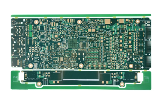
Help Center  
Sending a message
Open Hours:9:00-21:00 (GMT+8)
Service hotlines

9:00 -18:00, Mon. - Fri. (GMT+8)

9:00 -12:00, Sat. (GMT+8)

(Except Chinese public holidays)

X

Assembly Enquiry

Upload File

Instant Quote

x
Upload File

Comprehensive Multilayer PCB Services

PCBasic can meet all your PCB manufacturing needs, from single-layer to 32-layer boards. With over 15 years of industry experience, our team is skilled in multi-layer circuit board design and production, providing you with professional support. We offer free samples to ensure quality before mass production. For bulk orders, you can also enjoy exclusive discounts. This article outlines the key stages of PCB production to give you a clearer understanding of our service capabilities.

PCB Layer Introduction

Double-Sided Gold Finger PCB

Gold finger PCBs feature gold-plated edge connectors, offering excellent conductivity and wear resistance. They ensure stable signal transmission during repeated insertions and are widely used in smartphones, smart wearables, and communication devices.

Double-Sided PCB

Double-sided PCBs are commonly used in industrial control applications. They can be designed for specific functions like temperature control or as general-purpose programmable boards supporting secondary development. Typical uses include PLCs, relays, motors, and sensors, enabling automation functions such as data collection, speed control, and communication.

6-Layer PCB

6-layer PCBs add two signal layers to a 4-layer structure, usually consisting of outer layers, two internal signal layers, and power/ground planes. This design optimizes routing, reduces electromagnetic interference (EMI), and provides stable performance in high-speed communication systems.

8-Layer PCB

8-layer PCBs include four signal layers and four plane layers, delivering excellent EMC performance. With optimized layout and shielding, they provide sufficient wiring space and high reliability, making them ideal for high-speed, high-density applications such as computer motherboards.

12-Layer PCB

12-layer PCBs are widely used in automotive electronic systems, featuring high temperature and pressure resistance with excellent thermal stability. With advanced materials such as gold plating and resin filling, they maintain ±10% impedance control accuracy even at 288°C. Compared to 8- and 10-layer boards, they offer better performance at a slightly higher cost.

14-Layer PCB

14-layer PCBs are high-density multilayer boards, commonly used in satellite systems, front-end amplifiers, memory modules, SAN storage, and communication equipment. When stable signal layers or special shielding structures are required, 14-layer PCBs are often the preferred solution.

20-Layer PCB

20-layer PCBs are used in medical devices, communication, aerospace, and high-speed computing. They offer stable signal transmission, good EMC, and heat dissipation, with higher reliability than 16- and 18-layer boards.

24-Layer PCB

24-layer PCBs are advanced multilayer designs about 5.5 mm thick, with stable dimensions, strong grounding and power structures, and reliable performance. Their optimized stack-up and HDI compatibility suit high-density applications, while low-loss dielectric materials ensure excellent signal integrity.

Our 6 Core PCB Advantages

Excellent Signal Integrity

Multilayer design and optimized routing reduce crosstalk and noise, ensuring stable high-speed transmission for high-frequency circuits.

Flexible Layout

Layer count and structure can be flexibly adjusted to meet different design needs, from simple single-layer to high-density multilayer boards, achieving optimized layout and wiring.

High Reliability

Premium materials combined with precision processes and strict testing ensure long-term stability and durability, even in harsh environments.

High-Density Routing Support

Multilayer structures provide more routing space, enabling complex designs within compact sizes, supporting miniaturization and high integration.

High-Speed Performance

Optimized stack-up and impedance control ensure smooth transmission of high-speed and RF signals, ideal for 5G, communication, and radar applications.

Strong Environmental Resistance

Excellent resistance to heat, humidity, and vibration, making PCBs suitable for automotive electronics, industrial control, and aerospace under demanding conditions.

Our PCB Manufacturing Capability

Advanced processes enable flexible layers and materials, ensuring precise, high-density, and reliable PCB production.

Ltem
Capability
Process Details
Layers
2-32 layer PCBs
Number of PCB layers as defined in the design file.
Material Types
FR-4, high-Tg FR-4, aluminum substrates
FR-4 (standard, high-Tg, halogen-free) / aluminum substrates (insulated metal base).
Solder Mask
Taiyo / Guanghua / Rongda
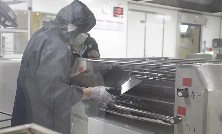
Solder mask quality directly affects PCB durability and final product performance.
Max Size
680 x 1200 mm
Max production size: double-sided PCB 680 x 1200 mm; 4- and 6-layer PCB 680 x 640 mm.
Board Thickness Range
0.4 - 2.0 mm
Standard PCB thickness options: 0.4 / 0.6 / 0.8 / 1.0 / 1.2 /1.6 / 2.0 - 3.0 mm.
Outline Accuracy
±0.15 mm
CNC routing tolerance ±0.15 mm; V-cut outline tolerance ±0.15 mm.
Thickness Tolerance (≥1.0 mm)
±10%
Influenced by production factors (plating, solder mask, surface finish), typically positive tolerance.
Thickness Tolerance (<1.0 mm)
±0.1mm
Influenced by production factors (plating, solder mask, surface finish), typically positive tolerance.
Min Trace/Space
4 mil trace / 4 mil spacing (0.1 mm)
Min line width and spacing 4 mil; best ≥ 4 mil.
Min Hole Size
0.2 mm
Min drill hole size 0.2 mm; recommended ≥ 0.2 mm.
Min Annular Ring
4 mil (0.1 mm)
Min annular ring 4 mil; best ≥ 4 mil.
Finished Copper Thickness
35 µm / 70 µm / 105 µm (1 oz / 2 oz / 3 oz)
Thickness of copper foil after plating. Options: 1-3 oz.
Finished Hole Size (PTH)
0.25-6.5mm
Plated through-holes are smaller than drill size due to copper plating.
Hole Tolerance (Drill)
±0.075 mm
Example: For a 0.6 mm drill, finished hole size may be 0.525-0.675 mm.
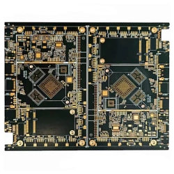
Solder Mask Colors
Green / Red / Blue / Black/ White / Purple...
Multiple solder mask color options available.
Min Silkscreen Line Width
≥0.15 mm
If less than 0.15 mm, text may appear blurred or unclear.
Min Silkscreen Text Height
≥0.8 mm
If less than 0.8 mm, text may appear broken or incomplete.
Sillkscreen Aspect Ratio
1:5
Proper aspect ratio ensures better manufacturability.
Clearance Between Trace and Outline
≥0.3 mm (12 mil)
For PCBasic production, the distance between trace and board outline should be ≥0.3 mm; for V-Cut panels, the distance from trace to V-Cut centerline should be ≥0.4 mm.
Panelization - No-Gap Panel
0 mm gap
For delivery panels, spacing between neighboring boards can be 0 (must be defined in the file).
Panelization - With Gap
1.6 mm
For panels with gaps, spacing should be ≥1.6 mm, otherwise edge milling is difficult.
PCB Outline Edge Milling
0.3 mm - 0.5 mm
Standard edgemilling tolerance is 0.5 mm; special requirements must be specified in advance.
Copper Thieving Method by Fabricators
Copper thieving / mesh
Fabricators may add copper thieving to reduce etching imbalance. Customers designing solder pads must consider this.
Defining Slots in CAD Software
Drill drawing layer
If the PCB contains many plated or non-plated slots, please define them in the Drill Drawing layer.
Window Layers in Protel/DXP Software
Solder mask layer
Avoid errors by defining solder mask openings in the solder mask layer, not in the paste layer.

PCB Application Fields

Covering diverse industries from consumer electronics to aerospace, driving global electronic innovation.

Aerospace

High-layer PCBs ensure reliable performance in flight control, satellite communication, and radar systems.

Automation

Multilayer PCBs power control panels, PLCs, and motor drives with stable, long-lasting performance.

Automotive

12- and 14-layer PCBs support ECUs, ADAS, battery management, and in-vehicle electronics.

Medical & Dental

20-layer PCBs enable precision and reliability in MRI, CT, ultrasound, and dental equipment.

Consumer Electronics

HDI and multilayer PCBs are used in smartphones, tablets, and wearables for compact, high-performance designs.

Robotics

24-layer PCBs drive AI cores, power modules, and sensors for advanced robotic systems.

PCB Assembly Machines

Drilling

Plating

Stripping

International Quality Certifications

Certified with ISO 9001, ISO 13485, IATF 16949, and more to ensure compliance with global standards.

High-Efficiency Production

Supports rapid delivery for small batches, with manufacturing completed in as fast as 24 hours to meet urgent deadlines.

One-Stop Service

15+ years of PCB/PCBA experience, covering design, prototyping, mass production, and assembly with full-process integrated solutions.

Advanced Technology Assurance

In-house intelligent production management system combined with a professional R&D team ensures high precision and reliability.

Global Logistics Network

Partnerships with DHL, FedEx, UPS, SF Express, and EMS for fast, safe, and secure worldwide delivery.

Professional Engineering Support

Free technical consulting and DFM analysis with 24/7 one-on-one service to help optimize product design and quality.

Key PCB Manufacturing Processes

Each step in the PCB manufacturing process adheres to strict inspection standards.

01File Review

Before production begins, we perform a comprehensive review of the design files provided by the customer (e.g., Gerber files) to ensure the integrity and manufacturability (DFM) of the PCB design. We also generate the necessary drill files, artwork files, and other production tools to ensure the accuracy and efficiency of subsequent processes.

02Inner Layer Fabrication

For multi-layer PCB production, inner layer fabrication is a crucial step. We use advanced photo imaging technology to precisely transfer the circuit pattern onto the copper-clad laminate, and chemically etch away excess copper to form the circuit pattern. AOI (Automated Optical Inspection) is then used to inspect 100% of the inner layer, ensuring no open circuits, shorts, or other defects.

03Drilling

We use high-precision CNC drilling machines to process through-holes, blind vias, and buried vias, ensuring precise hole locations and dimensions that meet design requirements. The cleaning process after drilling further removes residue inside the holes, laying a solid foundation for the subsequent via plating process.

04Through-Hole Plating

Through-hole plating is a core process for achieving interlayer electrical connections. We first use chemical copper deposition to deposit a conductive copper layer inside the holes, followed by electroplating to thicken the copper layer, ensuring the reliability of electrical performance and mechanical strength. We strictly control the plating thickness to meet international standards.

05Outer Layer Fabrication

The outer layer fabrication determines the final circuit pattern of the finished PCB. We use high-precision exposure technology and electroplating to transfer the circuit pattern onto the outer layers, followed by etching to remove excess copper foil. Once complete, all outer layers undergo AOI inspection again to ensure every PCB meets the design requirements.

06Solder Mask Application

Applying a solder mask to the PCB surface effectively protects the circuit areas and prevents soldering short circuits. We use automated coating equipment and precise exposure technology to ensure the solder mask ink is evenly applied, with precise opening for the soldering areas. After high-temperature curing, the solder mask layer provides excellent wear resistance and insulation properties.

07Surface Finish

To enhance the solderability of the PCB and protect exposed surfaces, we offer a variety of surface finish processes, including Hot Air Solder Leveling (HASL), Electroless Nickel Immersion Gold (ENIG), Immersion Tin, and OSP (Organic Solderability Preservative). Each process meets international standards to fulfill different application requirements.

08Electrical Testing

Before shipment, each PCB undergoes a comprehensive electrical test, including continuity and insulation checks. We use advanced flying probe or bed-of-nails test equipment to ensure that all electrical connections meet the design requirements, providing customers with stable and reliable products.

09Final Inspection

Once production is complete, we conduct a final inspection of the PCB's appearance and functionality to ensure there are no defects.

10Packaging

The PCBs are then packaged using anti-static bags, foam, and other materials to protect them from electrostatic discharge and physical damage. Finally, the PCBs are sealed in protective bags, labeled, and packed in outer cartons with cushioning materials to ensure safety and stability during transportation.
X

Cooperation Cases / Customer Testimonials

Thanks to 15+ years of effort and innovation in electronics, PCBasic has become one of the leading PCB & PCBA manufacturers in Shenzhen, China.

We tested multilayer PCBs from PCBasic, and their reliability was outstanding. Even under intensive testing, the boards remained stable. The production yield was very high, and the team kept us updated at every stage, making the entire process transparent and efficient.

Michael Johnson

PCBasic supplied us with 20-layer PCBs, and the quality of each batch was highly consistent with almost no variation. The stack-up design was precise, and the dimensions matched our drawings perfectly. Their engineering team proactively discussed details before production, which gave us full confidence in the outcome.

Anna Müller

We purchased 14-layer and 18-layer PCBs, and the performance exceeded our expectations. The boards were very stable, highly reliable, and passed all inspections without defects. The customer support team responded quickly and provided professional solutions to our technical questions, making the collaboration very smooth.

James Smith

We received 24-layer PCBs, and the workmanship was impressive. The pads and traces were neatly arranged, showing excellent precision. Delivery was on time, and throughout production, PCBasic’s engineers gave us valuable suggestions that helped optimize our design and improve production efficiency.

Dmitry Ivanov

Frequently Asked Questions

What is the difference between single-layer and multilayer PCBs?-
A single-layer PCB has only one layer of copper, with a simple structure and low cost, but limited wiring density. A multilayer PCB consists of multiple conductive and insulating layers stacked together, enabling higher wiring density, better signal integrity, and stronger electromagnetic compatibility, making it suitable for complex and high-speed circuit designs.

What are the advantages of multilayer PCBs?

+
The advantages of multilayer PCBs include high wiring density, good signal integrity, low electromagnetic interference, strong reliability, compact size, support for high-frequency and high-speed transmission, and suitability for high-end electronic products.

What are the disadvantages of multilayer PCBs?

+
The main disadvantages are complex manufacturing processes, longer production cycles, higher costs, difficulty in repair and rework, and higher requirements for design and manufacturing precision.

What are multilayer PCBs typically used for?

+
Multilayer PCBs are widely used in smartphones, servers, communication equipment, medical electronics, automotive electronics, aerospace, and military electronics where high performance and reliability are required.

Can multilayer PCBs withstand high power and high temperature?

+
Yes. Multilayer PCBs use high-temperature resistant substrates (such as FR4 and polyimide) and are designed with optimized copper thickness and thermal management to handle high-power and high-temperature environments. Specific performance depends on material selection and design processes.

What is the maximum number of layers PCBasic can provide for multilayer PCBs?

+
PCBasic can manufacture multilayer PCBs with up to 32 layers, meeting the needs of high-end electronic devices for high-density routing and signal integrity.

Does PCBasic provide design support for multilayer PCBs?

+
Yes, PCBasic offers comprehensive design and engineering support, including stack-up design, signal integrity analysis, and power network optimization, helping customers achieve more efficient and reliable PCB designs.

Does PCBasic provide testing services for multilayer PCBs?

+
Yes, PCBasic provides full testing services, including AOI inspection, flying probe test, X-Ray inspection, and functional testing, ensuring every multilayer PCB meets strict quality and reliability standards.

Launch Your Project at PCBasic

PCB Layer Solutions

Phone

wechat

E-mail

whats

Phone contact

+86-755-27218592

In addition, we've prepared a Help Center. We recommend checking it before reaching out, as your question and its answer may already be clearly explained there.

Wechat Support

In addition, we've prepared a Help Center. We recommend checking it before reaching out, as your question and its answer may already be clearly explained there.

WhatsApp Support

In addition, we've prepared a Help Center. We recommend checking it before reaching out, as your question and its answer may already be clearly explained there.