Electronic devices are constantly evolving towards smaller and faster designs. To meet this changing trend, packaging technologies for components are also continuously advancing. Among them, BGA (Ball Grid Array) packaging is one of the key technologies that drives miniaturisation and high-density design in advanced packaging. Nowadays, PCB BGA technology has become the mainstream packaging form for high-pin-count processors, memories, FPGAs, communication chips and other BGA chips, and is widely used. This article will introduce what BGA is, its importance, common BGA packaging types and the advantages of BGA technology.
What is BGA?
BGA is a surface-mount type of integrated circuit (IC) packaging form. It achieves electrical and mechanical connections with the PCB by using regularly arranged solder balls at the bottom of the package, unlike traditional packaging, which relies on side pins for connection. The solder balls of BGA are located at the bottom, which makes its pin density higher, thus enabling smaller size, lighter weight of the device, and is highly suitable for high-performance applications.
What is a BGA chip? A BGA chip refers to an integrated circuit packaged in the BGA form. These chips are usually applied in fields with extremely high requirements for speed, frequency and heat dissipation, such as CPU, GPU and FPGA, etc.
Key features of BGA include:
Bottom solder ball array connection, significantly increasing I/O density
Strong solder ball self-alignment capability
Shorter electrical paths, lower signal delay, and higher integrity
Smaller package size
Different applications have different device size requirements, and BGA packages are available in various sizes. Common package sizesinclude:
BGA Pitch
Characteristics
Typical Applications
1.27 mm
Large solder balls, high reliability; suitable for low-density designs
Industrial control boards, older-generation processors
1.00 mm
Good thermal performance and stability; widely compatible
Mainstream consumer electronics, communication modules
0.80 mm
Better signal integrity; supports more compact routing
Extremely high process difficulty; requires top-tier fabrication equipment
High-end FPGAs, AI processors, advanced computing devices
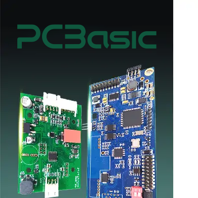
About PCBasic
Time is money in your projects – and PCBasic gets it. PCBasic is a PCB assembly company that delivers fast, flawless results every time. Our comprehensive PCB assembly services include expert engineering support at every step, ensuring top quality in every board. As a leading PCB assembly manufacturer, we provide a one-stop solution that streamlines your supply chain. Partner with our advanced PCB prototype factory for quick turnarounds and superior results you can trust.
Types of BGA Packages
The application requirements are constantly being refined, and to meet various needs, BGA PCB packaging has also developed multiple types. The common types include:
1.Plastic BGA (PBGA)
PBGA uses BT resin and glass fiber as the base material, with low cost and wide application. Due to its price advantage and stable performance, it is widely adopted in consumer electronics.
2.Ceramic BGA (CBGA)
CBGA uses multi-layer ceramic substrates and has excellent thermal stability and mechanical strength, making it suitable for high-reliability applications such as automotive electronics.
3. Film BGA (TBGA)
TBGA uses flexible films as the base material and supports bonding or flip-chip interconnection methods. Its structure usually has cavities, with excellent heat dissipation performance.
4.Miniature BGA (uBGA)
uBGA is extremely small in size and can significantly reduce the PCB board area. It is often used in high-speed storage modules.
5. Fine-pitch BGA (FBGA / CSP)
FBGA (also known as chip-scale packaging CSP) has very small solder ball pitches, usually ≤0.8 mm. Its packaging size is almost the same as the chip itself and is widely used in compact devices such as mobile phones and cameras.
Advantages of BGA
Higher PCB space utilization:The advanced PCB BGA manufacturing capability can fully leverage the compact advantages of BGA packaging. The bottom BGA pads connection is conducive to achieving a higher density PCB layout.
Excellent heat dissipation and electrical performance:Heat can be effectively conducted through the ball array in the BGA PCB design, making heat dissipation much easier. By optimizing the pad design, coating thickness, and BGA package sizes, it is possible to ensure that the BGA maintains stable electrical and thermal performance even under high-speed operation.
Higher solderingquality and production yield:Most BGA packages have relatively large solder balls. This large-scale solderingis more convenient and can increase the production speed and yield of the PCB. The self-aligning characteristic of the solder balls also helps to improve the solderingsuccess rate.
Greater mechanical reliability:The BGA packaging uses solid solder balls, eliminating the problems of traditional pins that are prone to bending or breaking.
Cost advantage:Higher yield, better heat dissipation capabilities, and smaller board footprint all contribute to reducing the overall manufacturing cost.
Applications of BGA
BGA has high density and excellent performance and is widely applied. It is commonly used in:
Microprocessors, graphics processors
DDR / DDR4 / DDR5 memory modules
FPGAs, DSPs
Smartphones, tablets, wearable devices
Industrial control equipment
Automotive ECU
High-speed communication equipment
Medical and aerospace electronics
Whether it is for high-speed signal transmission or demanding heat dissipation, or for miniaturization of equipment, BGA PCB is a very good choice.
PCBasic’s BGA Capability
PCBasic can support various BGA package sizes, ranging from the standard 1.0 mm and 0.8 mm, to the fine-spaced BGA with 0.5 mm and 0.4 mm. For high-performance processors or ultra-compact devices, we also offer:
HDI stack-up supporting microvia-in-pad
Laser drilling of blind holes
Via-in-Pad process with filling holes and copper plating
Impedance control wiring suitable for high-speed signals
Ultra-flat BGA pad surface finish
Since the solderingquality of BGA is highly dependent on the flatness of the pads, PCBasic prioritizes using ENIG as the surface treatment method in BGA design to ensure:
The surface of the pad is highly smooth.
Long-term reliable solderability.
The pads in the BGA area are of uniform height.
More stable solder ball formation and wetting effect.
This can effectively avoid common problems such as weld bridging, insufficient soldering, and poor wetting.
High-precision BGA chip mounting capability
The SMT production line of PCBasic is equipped with high-precision surface mount equipment, and it will ensure the assembly accuracy and consistency through the following processes:
SPI inspection after solder paste printing
Precisely aligned BGA component placement
Optimized reflow curves for different BGA types
High-precision reflow soldering furnace with closed-loop control
Complete BGA inspection and reliability verification
To ensure long-term performance reliability, PCBasic implements a strict inspection process for all BGA components in PCB assemblies:
X-Ray inspection of the internal quality of BGA solder balls
Analysis of void rate, solder ballstandoff height and alignment accuracy
Functional testing for processor-type circuits
Welcome to watch the following video to learn more about BGA assembly:
We use cookies to enhance your experience, analyze traffic, and provide personalized content. By clicking “Accept Cookies”, you agree to our Cookie and Privacy Policy.
Manage Cookie Preferences
We use cookies to enhance your browsing experience. Please review the details of each cookie category below and choose your preferences.
Strictly Necessary Cookies
These cookies are essential for the website to function properly and cannot be disabled. They are typically set in response to actions you take, such as logging in or adding items to your shopping cart.
Performance Cookies
These cookies help us understand how visitors interact with our website by collecting information about traffic and usage. This allows us to measure and improve the website’s performance.
Targeting/Advertising Cookies
These cookies are used to deliver
advertisements relevant to you and your interests. They may also limit the number of times you see an
advertisement and help measure the effectiveness of advertising campaigns.
In addition, we've prepared a Help Center.
We recommend checking it before reaching out, as your question and its
answer may already be clearly explained there.
✖
Wechat Support
In addition, we've prepared a Help Center.
We recommend checking it before reaching out, as your question and its
answer may already be clearly explained there.
✖
WhatsApp Support
In addition, we've prepared a Help Center.
We recommend checking it before reaching out, as your question and its
answer may already be clearly explained there.