SMT PCB Assembly Process - Surface Mount Technology
In the fast-paced world of electronics
manufacturing, surface mount technology (SMT) assembly is a pivotal innovation
that has reshaped the way we produce printed circuit boards (PCBs). This article
will take you on an in-depth look at the SMT assembly process as well as the
pros and cons!
What is SMT Assembly?
SMT's full name is "surface-mount
technology". SMT assembly is the method of correctly placing and soldering
the electronic components on the surface of the PCB using an automated machine.
With the development of smart technology today, SMT assembly has replaced the
traditional through-holes technology construction method of fitting electronic
components. SMT assembly allows to increase manufacturing automation so that it
reduces the manufacturing cost of PCBs greatly and leads to smaller boards.
About PCBasic
Time is money in your projects – and PCBasic gets it. PCBasic is a PCB assembly company that delivers fast, flawless results every time. Our comprehensive PCB assembly services include expert engineering support at every step, ensuring top quality in every board. As a leading PCB assembly manufacturer, we provide a one-stop solution that streamlines your supply chain. Partner with our advanced PCB prototype factory for quick turnarounds and superior results you can trust.
Advantages of SMT Assembly
1. High density SMT assembly:
Based on technology development, electronic products becomes smarter
and smarter, more and more sophisticated, it required that PCB assembly density
need to be greatly improved. And SMT assembly solved this problem
perfectly, it makes high density PCB assembly become possible.
2. Lower cost and faster produce speed:
Due
to the features of standardization, automation and holeless mounting,
smaller-size components mounting reduce a lot of cost than their larger
through-hole PCB, reduce drilling and increase the speed of produce.
3. Higher performance:
Using electronic
components with short-lead or no-lead, SMT assembly reduce parasitic
inductance and capacitance from the leads, improves the frequency and speed
performance of PCB. Keep the PCB and components out of heat effectively.
4. Reliable and stable:
Automated
production machines ensures that every connection of the components are
soldered well, SMT assembly improves the reliability and stability of
electronic products.
5.More
efficient use of pcb area:
Smaller electronic components and the technology of SMT
allow SMT assembly to have a better use on the PCB's surface area.
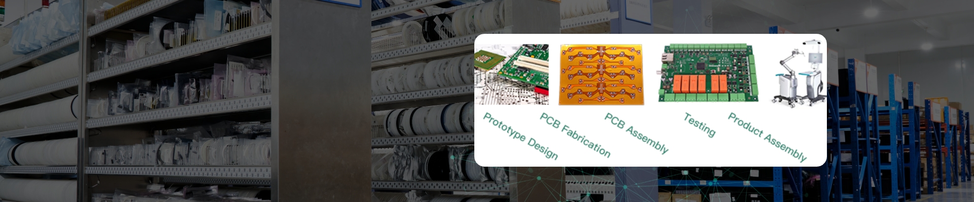
SMT PCB Assembly Processes
Normally, there are 16 processes in our company.
How Do Every Process Work?
First, purchase the electronic components
in need, IQC (income quality control) ensures every component is in good
quality and less errors in feeding.
Secondly, put them into Smart material
management system, every material has its own unique QR code to make sure
projects produced correctly. When the project starts, we will scan its QR code
to get the correct quantity and type of electronic components in need. It helps SMT
assembly process will place the correct electronic components on the PCBs.
Third, PCB fabrication. Produce the PCB following the files of PCB requests. Make sure that every components have correct pads on the correct places. PCB
fabrication. Produce the PCB following the files of PCB requests. Make sure
that every component has the correct pads in the correct places.
Fourth,stencil preparation; follow your PCB assembly files to make Stencils
for the SMT assembly process; we use a Laser Printer to dig holes in the
stencils in order to fit the pad on the PCBs. It will help the machines print
the solder and paste it on the PCBs' pads.
Fifth, program the SMT assembly machines to pick and place the
electronic components on the PCB correctly.
Sixth,feed preparation. To get the electronic components from the smart
management stock, put the feeds into SMT assembly machines by
scanning the QR code of each kind of electronic component; if you scan the
wrong QR code, the machines will give you an error. In this way, we have fewer
errors than other manufacturers.
Seventh, solder
paste printing; solder paste is a mixture of flux and tin; printing machines
print the solder paste on the PCB by using a squeegee. It is an important thing to design the thickness of stencil and
adjust the pressure of the squeegee, the thickness of solder paste on the PCB
depends on them. It will have a great influence on the next processes. So, it needs
to be scientific, refined and
standardized.
Eighth,SPI (solder paste inspection), One of the important processes
for SMT assembly. It is a machine to check the solder paste on the
PCB, Solder paste inspection machine adds a laser device for solder paste
thickness measurement, through checking Solder paste's printing volume, the height, area, flatness to make sure components soldered better.
Ninth,pick and place electronic components on PCBs through
high-speed SMT assembly machines. Each feeder is able to pick and
place the electronic components of 0201 and upward. During this step, SMT
assembly machines pick the correct components and place them on the PCBs
accurately following the program. This process enables fully automated assembly
and most SMT assembly machines can place over 40k components per
hour.
Tenth,inspect before reflow soldering, check whether the machine printed
solder paste well on the PCBs. if well, it will be sent to the next process, if
not, PCBs will be sent back to the last process until it passes the checking.
Eleventh,reflow soldering. During this step, the point is to melt the solder
paste and make the tin climb on the connections of components, then solidify.
After the PCBs leave the SMT assembly machine, it will be sent to
reflow oven. It has 10 different temperature zones, which will heat the PCBs and solder paste.
During hot gas soldering, the energy for
heating up the solder joint is transmitted by hot gas. This can be air or
nitrogen. In the reflow oven, PCBs will be heated to about 235-255℃, which is
higher than the melting point of solder paste. Within the temperature, you need
to consider the heat resistance of components. Solder paste is melted after
heating, and flux helps the tin climb on the connections of the components and
then solidify.
Twelfth, the
next step is AOI (Automated Optical Inspection). After reflow soldering, check
if there is no problem with the solder joint quality. With the development of
3D technology, it is more reliable to use 3D technology to check it than 2D
inspection. Cause there are more errors by 2D inspection, through 3D physical
optical imaging capabilities, 3D inspection allows to take more accurate
measurements and provides an inspection process. As the tin hardens, components
are affixed on PCBs, and the SMT assembly process is completed.
Thirteenth, X-ray inspection. After the SMT assembly, if the PCB has BGA and
other flat contacts, a matrix of solder balls or terminations will be placed on
the body of the component.
The size of the chip is also getting
smaller and smaller, and the pins of the chip become more and more, especially
the BGA chip that has appeared in recent years, because the pins of the BGA
chip are not distributed around the conventional design but are distributed on
the bottom of the chip.
There is no doubt that it is impossible to
judge the quality of solder joints through traditional visual inspection. AOI
can't inspect if the connections of components like BGA are soldered well, so
another method is needed to help with the inspection. X-ray equipment can
detect it by using the relationship between the penetrating power of X-rays and
the density of materials and using the property of different absorption to
distinguish materials with different densities.
Therefore, if the inspected object is
broken, the thickness is different, and the shape changes, the absorption of
X-rays is different, and the resulting image is also different, so a
differentiated black and white image can be generated.
Fourteenth, leaning
and drying. There are some oil and dirt in the whole production process and
they may lay on the surface of the PCB, so the PCB needs to be cleaned and dried before next process.
For example, soldering paste leaves behind some amount of flux, while human
handling can transfer oils and dirt from fingers and clothing to the surface of
the board.
Fifteenth, SMT
QA. It is the last step of the SMT assembly process. QA (quality assurance). In
this step, we check the PCBs again and test the PCB to test the result of the
SMT assembly.
Sixteenth, anti-static packaging. Cause some electronic components are easily
damaged by static electricity, preventing static electricity from them, and
Anti-static packaging is necessary.
No matter how perfect your manufacturing
factory is, it still has some troubles in production. Some of these troubles
are caused by nature, the others occur due to manufacturing errors. Surface
Mount Technology Assembly (SMT assembly) is one of those
processes which experiences such errors, but almost all errors can be avoided.
Common Problems during SMT Assembly
1. Solder
Bridging
This phenomenon is caused by bridging
across two different components, then lead to electronic short. The reason is
that when printing the solder paste, it generates excess solder on pcb and
cause wrong soldering on the PCB pad. You could try to make stencil thinner to
see whether difference happens.
2. Solder
Balling
Due to excessive humidity in the SMT
assembly device, it creates these solder balls during the reflow solder
process. Those balls may lead to electronic disruptions and some big balls of
them will cause functional issues in PCB. Thus, necessary to reduce the
humidity and moisture in the devices and please clean the bottom of the stencil
as dirt may also build these solder balls.
3. Tombstoning
This error has another name: “Manhattan
Effect". It happens when one connection lead of electronic components
raise and much higher than another lead, looks like a tombstone on the ground.
Thus, this phenomenon got this name. Uneven heat distribution of solder paste
is one cause of warping. The other reason is that electronic components aren't
placed at correct positions.
4. False soldering
It seems to be soldered on the surface;
however, it is actually not soldered. When you test its function, sometimes it
can pass the test, and sometimes it cannot, and it will show you its bad
contact.
SMT PCB Assembly from PCBasic
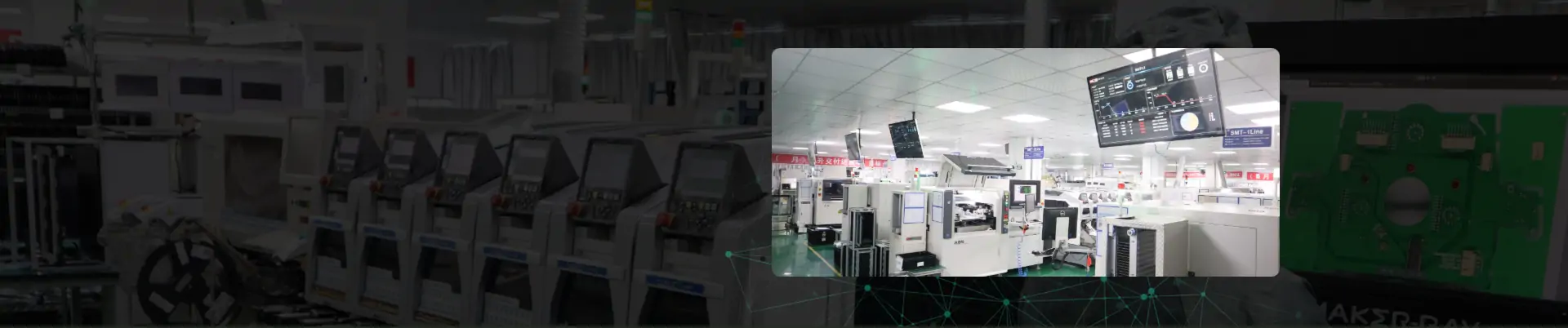
PCBasic is a global high-mix,
high-volume, and high-speed SMT PCB assembly manufacturer with more than 15+
years of industry experience. Equipped with 8 advanced SMT lines, we provide
efficient, stable, and traceable SMT assembly services to customers worldwide.
With factories in both Shenzhen and
Huizhou, we can flexibly handle small-batch rapid prototyping and large-scale
mass production. From SMT processing to component sourcing, stencil
manufacturing, and quality inspection, we offer full-process solutions to
accelerate delivery and ensure quality.
Why Choose PCBasic for Your SMT Assembly?
Professional SMT Manufacturing
Capabilities
• 8 SMT production
lines to support flexible order volumes
• Shenzhen factory
for small-batch quick-turn services
• Huizhou factory
for large-volume production
• In-house stencil
factory with stencil delivery in as fast as 1 hour
• In-house fixture
production for complex SMT needs
Efficient Material Management System
• One-click BOM
import with automatic quotation generation
• Intelligent
central warehouse for fast material turnover
• All components
are 100% original and genuine, ensuring reliability and supply stability
Strong Engineering & Project Support
• 10+ years of PCB
design and project management experience
• Industry-academia
collaboration with PhD teams, enabling advanced and complex SMT solution
development
Certified Quality Assurance
• Certified with
ISO13485, IATF 16949, ISO9001, ISO14001, and UL
• ANational
High-Tech Enterprise & IPC member
• Holder of 20+
patents in quality inspection and production management systems
• Full range of
testing equipment: AOI, X-ray, flying probe, and more to ensure SMT quality
Reliable Technical Support
• Dedicated teams
in engineering, quality, and IT working in sync
• 24/7 technical
response to support your project efficiently
We use cookies to enhance your experience, analyze traffic, and provide personalized content. By clicking “Accept Cookies”, you agree to our Cookie and Privacy Policy.
Manage Cookie Preferences
We use cookies to enhance your browsing experience. Please review the details of each cookie category below and choose your preferences.
Strictly Necessary Cookies
These cookies are essential for the website to function properly and cannot be disabled. They are typically set in response to actions you take, such as logging in or adding items to your shopping cart.
Performance Cookies
These cookies help us understand how visitors interact with our website by collecting information about traffic and usage. This allows us to measure and improve the website’s performance.
Targeting/Advertising Cookies
These cookies are used to deliver
advertisements relevant to you and your interests. They may also limit the number of times you see an
advertisement and help measure the effectiveness of advertising campaigns.
In addition, we've prepared a Help Center.
We recommend checking it before reaching out, as your question and its
answer may already be clearly explained there.
✖
Wechat Support
In addition, we've prepared a Help Center.
We recommend checking it before reaching out, as your question and its
answer may already be clearly explained there.
✖
WhatsApp Support
In addition, we've prepared a Help Center.
We recommend checking it before reaching out, as your question and its
answer may already be clearly explained there.


 About PCBasic


