Halogen-Free PCB: A Complete Guide
As global attention to carbon neutrality and green manufacturing deepens, when enterprises choose PCB materials, they no longer merely focus on performance indicators but pay more attention to the environmental friendliness of the materials. Halogen-free PCBs, with their outstanding thermal stability, excellent electrical performance and the ability to generate low-toxic gases when burning, are becoming the preferred solution for the next generation of electronic products.

Meanwhile, an increasing number of industry customers have explicitly put forward the hard and fast standard that PCBs must be halogen-free at the initial stage of the project. Whether it is smart wearables, communication base stations, or the control systems of new energy vehicles, the demand for halogen-free PCBs is growing rapidly and continuously. Selecting the right halogen-free PCB suppliers and manufacturing partners has also become an important part for enterprises to achieve green transformation and increase the added value of their products.
This article will systematically introduce to you what halogen-free is, the definition and advantages of halogen-free PCBs, as well as a reliable halogen free PCB manufacturers, to give your products an edge in future competition. First of all, let's get to know halogens.
What is Halogen?
Halogen is element in Group 17 of the periodic table, including fluorine, chlorine, bromine, iodine and astatine. In traditional PCB manufacturing, halogen-based flame retardants (especially brominated compounds) are often used to enhance fire resistance. However, when halogen-containing PCBs are exposed to high temperatures or burn, they will release toxic and corrosive gases, posing serious environmental and health risks. Therefore, in the electronics industry, especially in the field that emphasizes green production, PCB manufacturers are gradually turning to halogen-free materials.

In electronic products, halogen free means: the contents of chlorine and bromine in the material are each less than 900ppm, and the total halogen content does not exceed 1500ppm.
What is Halogen-free PCB?
Halogen-free PCB means printed circuit board with no halogen flame retardants in the substrate, specifically fluorine, chlorine, bromine, iodine, and astatine. This type of PCB adopts other types of flame-retardant systems, which not only provide excellent fire resistance performance but also do not bring the environmental risks of traditional halogen materials.

According to the JPCA-ES-01-2003 standard: Copper Clad Laminates (CCL) with chlorine (Cl) and bromine (Br) contents less than 0.09% wt (weight ratio) respectively are defined as halogen free PCB CCLs. (Meanwhile, total CI+Br ≤ 0.15% [1500 PPM])
Commonly used halogen-free PCB materials include modified epoxy resin, phenolic resin TU883 of TUC, DE156 of Isola, GreenSpeed® series, S1165/S1165M and S0165 of SYTECH or high Tg halogen-free FR4 materials. These materials can not only maintain good mechanical and electrical properties, but also eliminate the hazards caused by halogens.
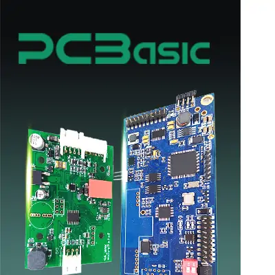
About PCBasic
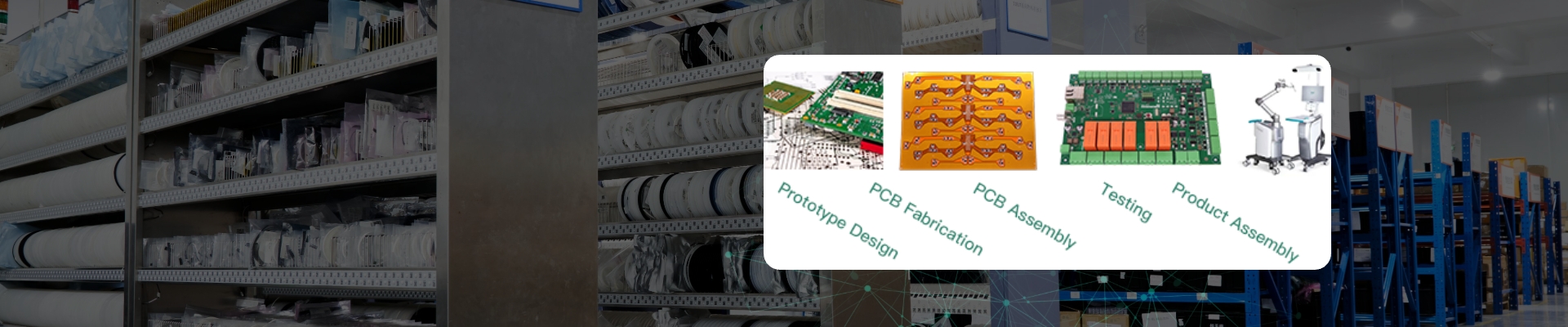
Time is money in your projects – and PCBasic gets it. PCBasic is the pcb assembly company that delivers fast, flawless results every time. Our comprehensive PCB Assembly Services include expert engineering support at every step, ensuring top quality in every board. As a leading PCB Assembly Manufacturer, we provide a one-stop solution that streamlines your supply chain. Partner with our advanced PCB Prototype Factory for quick turnarounds and superior results you can trust.
Why PCB Halogen Free?
Traditional PCBs use halogen-containing flame retardants (such as chlorine, bromine, etc.), which release harmful gases (such as dioxins and furans) during incineration, posing potential hazards to the environment and human health. Choosing halogen-free PCBs can ensure that these toxic substances are not produced during the electronic waste disposal process, meeting stricter environmental protection and safety standards. Meanwhile, environmental protection regulations around the world (such as the EU RoHS Directive) require the reduction of harmful substances. The restrictions on harmful substances in electronic products are becoming increasingly strict. Therefore, halogen-free PCBs have become a safer and more environmentally friendly option.
Relevant studies have shown that when halogen-containing flame retardant materials (like PBB, PBDE) are discarded and incinerated. They release dioxins (TCDD), benzofurans, etc. These substances are carcinogenic, produce a large amount of smoke, generate odors, and are accompanied by highly toxic gases. Once ingested by the human body, they cannot be excreted, seriously affecting health. This is also one of the important reasons for promoting the use of halogen-free PCBs.

It is understood that PBB and PBDE are basically no longer used in the PCB industry. However, apart from PBB and PBDE, brominated flame retardant materials, such as tetrabromodiphenol A and dibromophenol are more commonly used, and their chemical formula is CISHIZOBr4. Although such bromine-containing PCBs as flame retardants are not subject to any legal or regulatory restrictions, they will release a large amount of toxic gases (bromide type) and produce a lot of smoke when burning or in the event of an electrical fire. When tin spraying and component soldering are carried out on PCBs, the boards are affected by high temperatures (>200℃), which will release trace amounts of hydrogen bromide. As for whether toxic gases will also be produced, it is still under assessment at present.
At present, industries such as telecommunications, automobiles, consumer electronics and medical equipment are increasingly purchasing from halogen free PCB suppliers. Halogen, as a raw material, has a huge negative impact. It is imperative to ban halogen. PCBs halogen free are inevitable.
Halogen-Free PCB Performance
Before delving into halogen-free PCBs, it is essential to understand the principle and materials of halogen-free PCBs. Halogen free PCBs avoid the environmental risks of traditional halogen materials by using halogen-free materials (these materials have other types of flame retardant systems that can provide excellent fire resistance performance). Halogen-free PCB materials are usually mainly phosphorus-based or phosphorus-nitrogen-based compounds. During the pyrolysis process, these phosphorus-based resins will decompose to form metaphosphoric acid. This substance(metaphosphoric acid) has a strong dehydrating effect and will form a carbonized film on the surface of the resin, thereby isolating the air, extinguishing the fire source and achieving a flame-retardant effect. Phosphorus-nitrogen compounds release non-flammable gases during combustion, further enhancing the flame retardant performance of the resin system.
Common Halogen Free PCB Materials

Phosphorus-based Materials
Phosphorus-based is one of the commonly used halogen-free PCB materials, which is used to provide flame retardant performance. Phosphorus-based materials can release phosphorus when heated, which then reacts with the resin to form a protective carbonized layer, thereby preventing the spread of flames.
In LED lighting systems and power modules, a common phosphorus-based material is ammonium phosphate. When the temperature rises, ammonium phosphate decomposes to form metaphosphoric acid, which forms a protective carbonized film on the surface of the resin, effectively isolating air and extinguishing the flame, thereby achieving a flame-retardant effect.
Phosphorus-nitrogen Compounds
In addition to phosphorus-based materials, phosphorus-nitrogen compounds are also frequently used in halogen-free PCBs. These materials not only help enhance the flame retardancy of PCBs but also offer superior thermal stability.
Phosphorus-nitrogen flame retardants such as phosphorus-nitrogen compounds are usually used in high-power components of automotive electronics and industrial control systems. This type of material releases non-flammable gases such as nitrogen during the combustion process. These gases can effectively suppress the spread of flames, ensuring the safety and reliability of the equipment in high-temperature environments.
High-temperature Resin System
High-temperature resin systems, such as high Tg epoxy resins, are typically used in halogen-free PCBs. These resins can offer excellent heat resistance, mechanical stability and electrical properties, making them highly suitable for applications involving high power or extreme environments.
In fields such as automotive electronics and industrial power modules that require high-temperature resistance, these materials can still maintain stable electrical performance even in high-temperature environments. The glass transition temperature (Tg) of these resins is usually above 170°C, enabling halogen-free PCBs to operate in high-temperature environments without affecting electrical and mechanical properties.

Halogen-free FR4 material
FR4 is a widely used substrate for PCBs and is traditionally made of epoxy resin and glass fiber. Halogen-free FR4 materials typically use modified epoxy resins such as DE156 or GreenSpeed®. These modified resins have removed the halogen components in traditional FR4 and maintained the excellent electrical insulation, mechanical strength and thermal stability that traditional FR4 possesses. This material is widely used in fields such as consumer electronics, LED lighting, and electric vehicle battery management systems, ensuring that products maintain high performance while being environmentally friendly.
The use of halogen-free PCB materials not only effectively reduces the emission of harmful substances but also ensures that products comply with increasingly strict global environmental protection requirements, such as the RoHS (Restriction of Hazardous Substances Directive) standard.
Performance of Halogen Free PCB
Having understood the materials of halogen-free PCBs, let's now learn about the performance of halogen-free PCBs together! The performance of halogen-free PCBs is comparable to that of traditional halogen-containing PCBs, but its advantages lie in being more environmentally friendly, safer and in compliance with global environmental protection standards. Halogen-free PCBs have the following properties:

1. Flame retardant
The most notable advantage of halogen-free PCBs is their excellent flame retardant performance. Halogen-free PCB materials can effectively prevent the spread of flames, ensuring the stability and safety of PCBs in high-temperature or extreme environments.
2. Electrical performance
The electrical performance of halogen-free FR4 PCBs is comparable to that of traditional FR4 PCBs. Halogen-free PCB materials can provide excellent insulation and signal transmission performance, ensuring good electrical performance while reducing negative impacts on the environment, meeting environmental protection and industry standards.
3. Mechanical stability
Halogen-free PCBs can remain stable when subjected to vibration, shock or temperature changes, and are particularly suitable for applications that require high reliability, such as automotive electronics and industrial control systems.
4. Thermal management
Halogen-free PCBs have excellent thermal management performance, which can effectively conduct heat away from key components, prevent equipment damage caused by overheating, and thereby increase the service life of the equipment. It is particularly suitable for high-power applications such as LED lighting systems, power modules and automotive electronics.
At present, most halogen free PCB materials are mainly phosphorus-based and phosphorus-nitrogen-based materials. When the phosphorus-containing resin is burned, it is decomposed by heat to generate metaphosphoric acid, which is extremely dehydrated, so that a carbonized film is formed on the surface of the polymer resin, and the burning surface of the resin is isolated from the air, so that the fire is extinguished and the flame retardant effect is achieved. Polymer resins containing phosphorus and nitrogen compounds produce incombustible gas when burning, which helps the resin system to be flame retardant.
Characteristics of Halogen Free PCB

Insulation of Halogen Free PCB material
Because P or N is used to replace halogen atoms, the polarity of molecular bond segments of epoxy resin is reduced to some extent, thus improving the insulation resistance and breakdown resistance.
Water absorption of Halogen Free PCB material
Halogen free PCB has fewer foxes of N and P in nitrogen-phosphorus redox resin compared with halogen, and its probability of forming hydrogen bonds with hydrogen atoms in water is lower than that of halogen materials, so its water absorption is lower than that of conventional halogen flame retardant materials. For PCB material, low water absorption has a certain influence on improving the reliability and stability of materials. Reducing the water absorption rate of the Halogen Free PCB material will have a certain impact on the material in the following aspects:
(1) Improve the reliability of halogen free PCB materials.
(2) Improve the stability of materials in PCB manufacturing process.
(3) Improve the CAF performance of the halogen free PCB material.
Dielectric constant
The factors affecting the dielectric constant of materials are mainly determined by the following factors: dielectric constant of glass fiber, epoxy resin and filler. As P or N is used to replace halogen atoms, the polarity of the whole epoxy resin will be reduced to a certain extent, so the electrical insulation of halogen-free epoxy resin will be better than that of halogen-based epoxy resin, and the dielectric loss will be lower than that of conventional materials.
Thermal stability of Halogen Free PCB material
The content of nitrogen and phosphorus in Halogen Free PCB is higher than that of halogen in common halogen-based materials, so its monomer molecular weight and TG value have increased. When heated, its molecular mobility will be lower than that of conventional epoxy resin, so the thermal expansion coefficient of Halogen Free PCB material is relatively small.
Compared with halogen-containing PCB, halogen free PCB have more advantages, and it is the general trend that halogen free PCB replace halogen-containing PCB.
ion migration (CAF) resistance
Ion migration in the substrate mainly comes from the following three aspects:
(1)Copper metal cations.
(2)Halogen anion.
(3)Ammonia cation.
Among them, halogen ions can not only migrate themselves, but also cooperate with divalent copper ions to increase the possibility of ion migration. Halogen-free materials eliminate the possibility of remaining hydrolyzable halogen in the synthesis process, thus improving the ion migration resistance. At the same time, due to the low water absorption of halogen-free epoxy resin, the source of ion generation is reduced to some extent, thus improving the CAF resistance of the material.
Halogen Free PCB has been used more and more in the environment with environmental protection and lead-free requirements. First of all, Halogen Free PCB is used in fields with high environmental protection requirements such as medical treatment, followed by more and more applications in mobile phones and automobiles. Recently, more and more enterprises of electronic products pay more attention to the application of Halogen Free PCB. For example, Sony of Japan put forward the requirements of using halogen-free multilayer boards and HDI boards in its products. Then, I’d like to share an excellent and reliable halogen PCB manufacturer with you - PCBasic.
PCBasic’s Halogen Free PCB Manufacturing

Experience in Halogen Free PCB Manufacturing Process
1. Lamination
Lamination parameters may vary from company to company because of the PCB materials. Taking the above-mentioned SYTECH substrate and PP as the multilayer board, in order to ensure the full flow of resin and good bonding force, it requires a lower heating rate (1.0-1.5℃/min) and multi-stage pressure coordination. In addition, in the high temperature stage, it requires a longer time, and the temperature of 180℃ should be maintained for more than 50 minutes.
2. Drilling machinability
Drilling condition is an important parameter, which directly affects the hole wall quality of PCB during processing. Halogen Free PCB increases the molecular weight and the rigidity of molecular bonds by using P and N series functional groups, thus enhancing the rigidity of materials. At the same time, the TG point of halogen-free materials is generally higher than that of ordinary copper clad laminate. Therefore, the drilling effect of ordinary FR-4 drilling parameters is generally not ideal. When drilling halogen-free plate, some adjustments should be made under normal drilling conditions.
3. Alkali resistance
Generally, the alkali resistance of Halogen Free PCB is worse than that of common FR-4. Therefore, special attention should be paid to the etching process and the rework process after solder resist, and the soaking time in alkaline stripping solution should not be too long, so as to prevent white spots on the substrate.
4. Halogen-free solder resist fabrication
At present, there are many kinds of halogen-free solder resist inks introduced in the world, and their performances are not much different from those of ordinary liquid photosensitive inks, and their specific operations are basically similar to those of ordinary inks.
Halogen free PCB has low water absorption and meets the requirements of environmental protection, and other properties can also meet the quality requirements of PCB. Therefore, the demand for halogen free PCB has been increasing.
Comparison of manufacturing performance

1. Etching
Because of the poor fluidity of halogen-free epoxy resin and the poor interpenetrating ability of copper foil interface, the peeling strength of copper foil of Halogen Free PCB is poor. Compared with conventional materials, halogen-free materials increase the pressing pressure in the pressing process in order to enhance the binding force between copper foil and resin, which leads to the deeper depth of part of copper embedded in the resin, which easily leads to the phenomenon of etching uncleanness in the etching process (the copper is exposed in the stars). In order to solve this problem, it is often improved by increasing the amount of wire width on the working negative and properly adjusting the etching rate.
2. Lamination
The content of nitrogen and phosphorus is higher than that of halogen in conventional halogen-based flame retardant materials, which leads to the increase of polymerization degree and molecular weight of polymer. Therefore, the molecular chain movement of halogen-free epoxy resin after heating is slower than that of conventional materials, which shows that the fluidity of halogen-free materials will be lower than that of conventional epoxy resin under the same conditions.
3. Drilling electroplating
Halogen free PCB material have higher Young's modulus, which increases the rigidity and brittleness of materials, because of the use of P and N series functional groups to increase the molecular weight and the rigidity of molecular bonds. At the same time, the TG point of halogen free PCB material is higher than that of conventional materials of the same type. Therefore, it is necessary to properly increase the rotation speed of the drill and reduce the feed speed of the drill to ensure the roughness of the hole wall when mechanical drilling is carried out. In the process of horizontal deslagging, it is necessary to prolong the expansion reaction time, increase the roughness of the hole wall and improve the bonding force between electroplated copper and the hole wall according to the characteristics of halogen-free materials.
4. Laser drilling
Comparing halogen-free materials with conventional materials under the same technological conditions of laser drilling, it is found that the hole wall roughness and verticality of halogen-free materials after drilling are not as good as those of conventional materials, which can be more prominent after electroplating. Therefore, it is necessary to appropriately increase the pulse energy and quantity of laser drilling of halogen free PCB material.
5. Solder resist fabrication
Halogen-free solder resist ink has a high solid content of curing agent (take Company C as an example: conventional halogen-free material is 15% and 30%), so its viscosity is high and fluidity is low. In printing, it is necessary to increase the pressure of scraper and adjust the mesh number of screen. Under certain conditions, a certain amount of diluting solvent can be used for dilution to increase the fluidity of ink.
6. Impedance fabrication
At low frequency (less than or equal to 1.5GHZ), the dielectric constants of the two materials are less affected by thermal shock and decrease to some extent. When the test frequency reaches a certain value (1.8GHZ), the two materials are obviously different under the influence of thermal shock. The dielectric constant of halogen-free materials decreases obviously and fluctuates slightly after thermal shock, while the dielectric constant of conventional materials increases greatly with the increase of thermal shock times.
Therefore, halogen-free materials can avoid the influence of multiple thermal shocks on the dielectric constant of the materials in the PCB process, which is beneficial to the control of characteristics or differential impedance. Halogen Free PCB material have higher dielectric constant, and the dielectric thickness after lamination is thicker than that of conventional materials, so the impedance value will be increased to a certain extent when impedance control, especially the control of characteristics and differential impedance. When designing the wire width, appropriate compensation is needed.

Choosing PCBasic as Your Reliable Halogen Free PCB Manufacturer!
As a leading halogen-free PCB manufacturer, PCBasic is your reliable partner. We focus on manufacturing halogen-free PCBs that comply with global environmental regulations such as RoHS and WEEE, ensuring your products are safe, durable and sustainable. Our advanced manufacturing processes and commitment to quality ensure that each PCB offers excellent thermal management, mechanical stability and electrical performance. Our factory is equipped with the most advanced facilities and is capable of handling all demands ranging from rapid prototyping, small-batch production to large-scale manufacturing.
As a reliable halogen-free PCB supplier, PCBasic offers customized solutions for a wide range of applications, including LED lighting, automotive electronics, and medical devices. We are committed to precisely and efficiently meeting your specific requirements.
Contact us immediately to learn about our halogen-free PCB solutions!