Global high-mix volume high-speed PCBA manufacturer
9:00 -18:00, Mon. - Fri. (GMT+8)
9:00 -12:00, Sat. (GMT+8)
(Except Chinese public holidays)
Global high-mix volume high-speed PCBA manufacturer
9:00 -18:00, Mon. - Fri. (GMT+8)
9:00 -12:00, Sat. (GMT+8)
(Except Chinese public holidays)
HomePage > Blog > Knowledge Base > 2 oz Copper Thickness in PCBs – A Complete Guide
In electronic manufacturing, the copper thickness on printed circuit boards (PCBs) is actually very important, but it is often overlooked. It directly affects how much current the PCB can carry, whether it can dissipate heat in time, and the overall reliability.
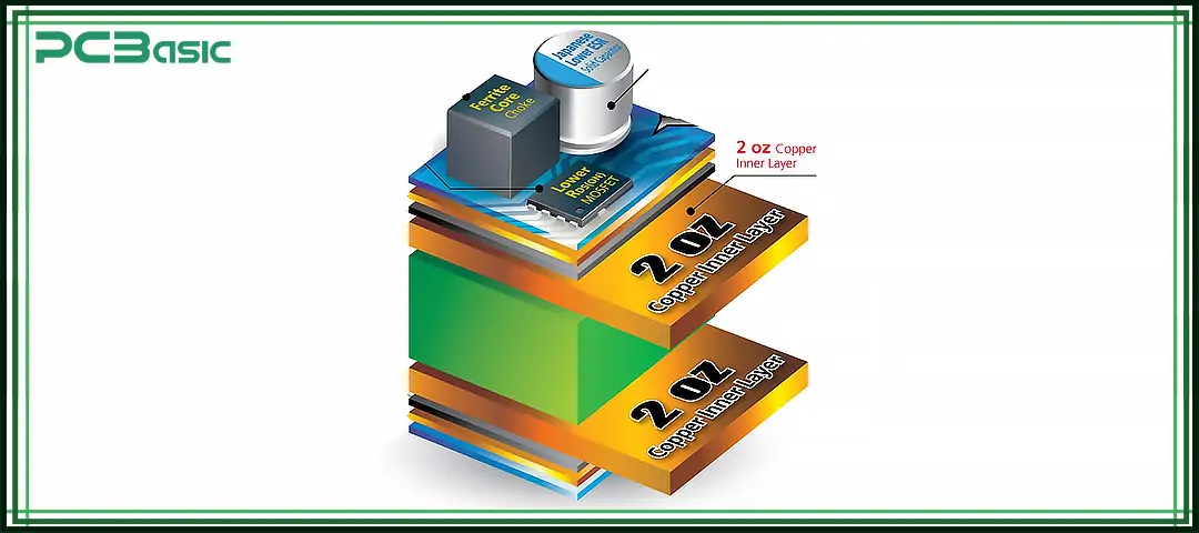
With the increasing power of electronic products, 2 oz copper thickness PCBs are being used more and more widely. Compared with the common 1 oz PCB, the 2 oz PCB can carry a greater current, has better heat dissipation performance, and stronger electromagnetic shielding capability. Therefore, it is particularly suitable for high-performance design.
However, it should be noted that there may be deviations in the thickness of copper during production and manufacturing. There may be a deviation of about ±10% from the starting copper thickness to the final finished copper thickness. Therefore, when designing and selecting the type, this factor must be taken into account.
This guide will give you a comprehensive understanding of 2 oz copper thickness PCBs: their definition, advantages, and the differences between them and 1 and 3oz copper PCBs in terms of electrical performance, heat dissipation capacity and manufacturing process, helping you find the right balance between performance and cost.

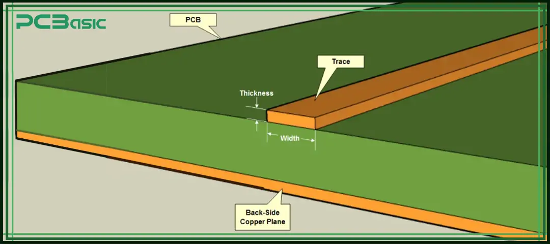
In the PCB industry, we do not directly use "microns (µm)" to represent copper thickness, but measure it by the weight of copper per square foot (oz/ft²). In other words, "oz" is actually a unit of weight, not a unit of thickness.
If you spread 2 oz copper over one square foot of PCB area, a thickness of approximately 70 microns (2.74 mils) will be achieved. This is exactly twice the standard 1 oz copper thickness, approximately 35 µm.
2 oz copper thickness PCBs are widely used in many situations that require high reliability and long service life. It can carry more current than a 1 oz copper PCB, dissipate heat faster and is more durable, thus being suitable for medium-to high-power and harsh environments. Common applications include:
In a power supply system, the current is usually quite large. If the copper layer is too thin, it is prone to overheat and even burn out. 2 oz copper thickness can carry current more stably, and therefore is often used in inverters, DC-DC converters, power distribution boards, etc.
The current and temperature resistance requirements for PCBs in electric vehicles and hybrid vehicles are very high. 2 oz copper PCBs are often used in EV chargers, battery management systems (BMS), and high-power motor drive modules.
High-brightness LEDs generate a large amount of heat. If the heat dissipation is not good, their lifespan will be greatly shortened. A 2 oz copper thickness PCB can quickly conduct heat away, so it is often used in LED drivers, high-power lamps and lighting applications that require good thermal management.
Equipment in industrial environments, such as motor controllers, high-power drives and control circuits of heavy machinery, often have to handle high currents. A 2 oz copper PCB can ensure long-term stable operation and reduce the risk of downtime.
In aircraft, spacecraft or military equipment, PCBs not only have to withstand large currents, but also resist extreme temperatures, vibrations and harsh environments. The 2 oz copper thickness offers higher mechanical strength and reliability, and thus is widely adopted.
Even in some smaller-sized devices, a relatively high current may be required, such as small power adapters, portable devices or audio power amplifier circuits. A 2 oz copper PCB can ensure a safe current-carrying capacity while maintaining a compact design.
All in all, 2 oz copper thickness has obvious advantages in both current transmission and heat dissipation performance, and thus has become the preferred choice for engineers and manufacturers in medium-to high-power circuits.

In PCB design, the reason why 2 oz copper thickness is increasingly favored by engineers and manufacturers is that it provides a good balance between performance and cost. Compared with the 1 oz copper PCB, it is obviously more powerful, and does not increase the manufacturing difficulty and cost as much as the 3 oz copper PCB.
In high-power circuits, the current is relatively large, and copper layers that are too thin or too light are prone to overheating or even burning out. The 2 oz copper thickness enables the same width of traces to carry more current while reducing the risk of overheating.
The thicker the copper layer is, the better the heat conduction ability will be. Applications that generate a lot of heat often have higher requirements for heat dissipation.
The wires of a 2 oz copper thickness PCB are more robust, less likely to break or delaminate, and more stable during soldering. This is particularly important for circuit boards that operate for long periods in high-temperature, vibrating or humid environments.
Under high load or long-term working conditions, the traces of the 2 oz copper PCB are less likely to burn out or degrade, which can significantly extend the product life and reduce maintenance costs.
If only 1 oz of copper thickness is used, wider traces are usually required when designing high-current circuits, which will occupy more space. The 2 oz copper PCB enables engineers to use a smaller trace width within a limited board space while still safely transmitting large currents.

Time is money in your projects – and PCBasic gets it. PCBasic is a PCB assembly company that delivers fast, flawless results every time. Our comprehensive PCB assembly services include expert engineering support at every step, ensuring top quality in every board. As a leading PCB assembly manufacturer, we provide a one-stop solution that streamlines your supply chain. Partner with our advanced PCB prototype factory for quick turnarounds and superior results you can trust.
In PCB design and manufacturing, using a 2 oz copper thickness must strictly follow the internationally recognized IPC standard to ensure the safety and reliability of the circuit board. These standards provide clear references for designers and manufacturers, ensuring that PCBS produced by different manufacturers all meet consistent quality requirements.
Common relevant standards include:
|
Standard |
Main Content |
Relation to 2 oz Copper Thickness |
|
IPC-2221 |
Design rules: trace width vs. current capacity |
Guides trace sizing for 2 oz PCBs |
|
IPC-6012 |
Performance specification for rigid PCBs |
Ensures reliability and consistency |
|
IPC-A-600 |
Acceptability standards, including copper checks |
Determines if 2 oz PCBs meet requirements |
|
IPC-2152 |
Charts for copper thickness vs. current capacity |
Confirms safe current levels for 2 oz PCBs |
Simply put, adhering to these IPC standards can ensure that 2 oz copper-thick PCBs meet international industry standards in terms of electrical performance, mechanical strength and service life, avoiding problems such as overheating, burning out or premature failure.
The copper thickness chart is an important tool used to convert the copper weight into the corresponding physical copper thickness. It can help PCB designers clearly understand the impact of copper layer thickness on current carrying capacity, heat dissipation performance and board surface layout. Below is a simplified copper thickness chart for reference:
|
Copper Weight |
Thickness (mm) |
Thickness (mil) |
|
0.5 oz |
0.0174 mm |
0.68 mils |
|
1 oz |
0.0348 mm |
1.37 mils |
|
2 oz |
0.0696 mm |
2.74 mils |
|
3 oz |
0.104 mm |
4.11 mils |
|
4 oz |
0.139 mm |
5.48 mils |
Through the copper thickness chart, PCB engineers can easily complete the conversion of copper weight to thickness during the PCB layout and manufacturing stages, thereby ensuring that the design meets the requirements of current carrying and heat dissipation.
When comparing the thickness of 2 oz copper with that of 1 oz and 3 oz, the differences and trade-offs between them can be clearly seen:
Copper Thickness Comparison
|
Copper Thickness |
Thickness (μm / mils) |
Advantages |
Disadvantages |
Typical Applications |
|
1 oz Copper |
~35 μm / 1.37 mils |
Low cost, mature process, widely used, supported by most fabs |
Limited current capacity, overheating under high load |
Consumer electronics (phones, PC motherboards), control circuits, and home appliances |
|
2 oz Copper |
~70 μm / 2.74 mils |
Higher current capacity, better heat dissipation, stronger, good balance of performance and cost |
Higher cost than 1 oz, stricter manufacturing requirements |
Power circuits, automotive PCBs (EV chargers, BMS), LED drivers, motor controllers, medium-power designs |
|
3 oz Copper |
~105 μm / 4.11 mils |
Heavy copper, very high current capacity, excellent reliability, ideal for harsh environments |
High cost, difficult to manufacture, longer lead time, limited fab capability |
Military electronics, aerospace, power distribution, industrial inverters, high-power equipment |
In PCB design, selecting the appropriate PCB copper thickness is a very crucial step. If the copper thickness is insufficient, it may lead to overheating, shortened lifespan or even circuit failure. If the copper is too thick, it will increase the cost and manufacturing difficulty. Therefore, when choosing the copper thickness of a PCB, we usually need to consider the following aspects comprehensively:
The amount of current is the primary factor for us to choose copper thickness. Designers will refer to the IPC-2152 standard to calculate the required trace width based on the projected current value in the circuit.
For high-power circuit boards, relying only on fans or heat sinks may not be sufficient. Copper itself has good thermal conductivity, increasing the thickness of copper can conduct heat away more quickly.
In small PCBs with limited space, designers often cannot infinitely widen the traces to carry current. At this point, using a 2 oz copper thickness or thicker copper layer can meet the current-carrying requirements within a limited area while keeping the board compact.
The 1 oz copper PCB is the cheapest, but it may not be reliable enough in medium-to high-power applications. Although the 3 oz copper PCB has stronger performance, it is costly and difficult to manufacture. In contrast, the 2 oz copper PCB strikes an ideal balance between performance and cost, meeting most current and heat dissipation requirements without overburdening manufacturing costs.
In some critical fields, such as aerospace, automotive and defense equipment, the reliability requirements for PCBs are extremely high. In many cases, regulations or customers will require at least 2 oz copper thickness to ensure that the circuit remains safe and stable in harsh environments.
All in all, choosing the appropriate copper thickness for a PCB requires taking into account the current size, heat dissipation requirements, board space, cost, and industry standards. For most medium-to high-power applications, a 2 oz copper PCB is often the most reasonable choice.
2 oz copper thickness maintains a good balance between current capacity, thermal performance and cost-effectiveness. It is commonly found in industries such as power electronics, automotive, LED lighting and aerospace, which have extremely high requirements for durability and reliability.
As long as designers understand the differences in copper thickness of 1 oz, 2 oz and 3 oz, they can make a more appropriate choice among performance, reliability and budget, making the circuit both safe and efficient.
If you are not sure which copper thickness to choose, you can refer to the IPC-2152 current-carrying charts, which is best to cooperate with experienced PCB manufacturers. Make sure your 2 oz copper PCB meets the design requirements and industry standards.

Assembly Enquiry
Instant Quote
Phone contact

+86-755-27218592
In addition, we've prepared a Help Center. We recommend checking it before reaching out, as your question and its answer may already be clearly explained there.
Wechat Support

In addition, we've prepared a Help Center. We recommend checking it before reaching out, as your question and its answer may already be clearly explained there.
WhatsApp Support

In addition, we've prepared a Help Center. We recommend checking it before reaching out, as your question and its answer may already be clearly explained there.