Global high-mix volume high-speed PCBA manufacturer
9:00 -18:00, Mon. - Fri. (GMT+8)
9:00 -12:00, Sat. (GMT+8)
(Except Chinese public holidays)
Global high-mix volume high-speed PCBA manufacturer
9:00 -18:00, Mon. - Fri. (GMT+8)
9:00 -12:00, Sat. (GMT+8)
(Except Chinese public holidays)
HomePage > Blog > Knowledge Base > Solderability Testing in Electronics: Methods, Standards, and Advanced Techniques
In modern electronics manufacturing, solderability testing is a key step to ensure product quality and reliability. As electronic devices continue to develop towards miniaturization, high performance and long service life, the requirements for solder joint quality are also getting higher and higher. Whether an electronic product can operate stably often depends on the reliability of each solder joint. If there are problems with the solder joints, even the most advanced design may fail prematurely due to poor connection, oxidation of the metal surface or insufficient wetting. Such problems not only lead to rework and scrapping, but also may cause sudden malfunctions of the products during use, resulting in higher economic losses and credibility risks.
Therefore, electronics manufacturers will incorporate solderability testing into their production processes to verify whether the pins of components, PCB pads, and various surface treatments have good soldering performance. Through this test, potential defects can be detected before final product assembly, preventing defective products from entering the next process and significantly reducing the risk of later rework and quality accidents.
This article will systematically introduce the relevant contents of solderability testing, including its basic definition, why it is so important in manufacturing, the scientific principles it relies on, the core testing methods commonly adopted in the industry, and the corresponding international standards (such as J-STD-002 and J-STD-003), and advanced evaluation techniques, including wetting balance testing.

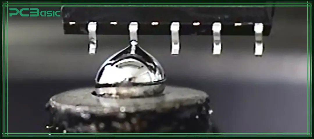
Solderability refers to the ability of a metal surface, such as the component lead, PCB pad or terminal, to be well wetted by molten solder and form a firm, uniform and continuous bond. Good solderability can ensure that the solder joints not only have sufficient mechanical strength but also provide stable electrical connections.
If solderability is poor, several issues usually occur: incomplete wetting, non-wetting, or dewetting. These problems are often caused by oxidation of the metal surface, contamination, excessive storage time, or improper surface treatment.
Therefore, before entering large-scale production, solderability testing must be conducted to confirm whether the surface of components or circuit boards can be reliably wetted by solder. In simple terms, solderability testing can prevent expensive losses caused by solder joint failure during actual use of products, reduce rework, and improve the overall quality of electronic assembly.
In the electronics manufacturing industry, the role of solderability testing is irreplaceable. As electronic products become increasingly complex and the requirements for reliability are higher, the quality of solder joints directly determines whether the entire product can operate stably. We can understand the importance of solderability testing from the following aspects:
If the necessary soldering testing is not carried out, the solder joints may have cold solder, open circuits or poor connectivity. These problems, at the very least, can cause unstable product performance, and at the worst, they can cause large-scale product recalls, resulting in huge economic losses.
Through solderability testing, it can be verified whether the metal surface can still be well wetted by solder after storage, transportation or environmental changes. This step ensures that the product remains reliable throughout its entire life cycle, not just being qualified at the time of leaving the factory.
Electronic components are not always in the best condition. Many devices will oxidize due to prolonged storage, leading to a decline in solderability. At this point, solderability testing can detect whether these components can still be used safely and prevent defective devices from being put into production.
Electronic manufacturing is not an arbitrary operation and must follow industry standards. For instance, both J-STD-002 (solderability requirements for component leads) and J-STD-003 (solderability requirements for PCB surface finishes) clearly define the testing methods and acceptance criteria. Adhering to these standards can ensure that the products meet the internationally recognized quality requirements.
Overall, solderability testing is not only a preventive measure to detect potential defects, but also a core stage to ensure the quality of the entire electronic manufacturing system. Solderability testing enables manufacturers to control risks at the early stage of production, avoid rework and accidents, and ultimately enhance the reliability and market competitiveness of the products.

Time is money in your projects – and PCBasic gets it. PCBasic is a PCB assembly company that delivers fast, flawless results every time. Our comprehensive PCB assembly services include expert engineering support at every step, ensuring top quality in every board. As a leading PCB assembly manufacturer, we provide a one-stop solution that streamlines your supply chain. Partner with our advanced PCB prototype factory for quick turnarounds and superior results you can trust.
The core of solderability lies in wetting, which is the process by which molten solder naturally spreads across a solid metal surface. This process does not occur randomly but is determined by the interfacial tension among the solder, flux and the metal surface. In other words, the quality of wetting directly affects whether the solder joints are firm and uniform.
To achieve reliable soldering, the following three basic conditions must be met:
1. Clean Surface: If there are oxides, grease, or dust on the metal surface, it will hinder the spreading of solder. The cleaner the surface is, the easier it is for the solder to wet, ensuring a good bond.
2. Active Flux: The function of flux is to remove the oxide layer on the metal surface and maintain surface activity during the soldering process, allowing the solder to spread smoothly. Without suitable flux, even if the temperature is sufficient, the solder may not be properly wetted.
3. Appropriate Temperature: If the temperature is too low, the solder cannot be fully melted, and the wetting will be poor. If the temperature is too high, it may damage the components or accelerate surface oxidation. Only when the temperature is controlled within an appropriate range can the solder flow and fully bond with the metal surface.
If any of these three conditions is not met, solderability will be greatly reduced and the reliability of the solder joints will also be affected. This is precisely why, in solderability testing, it is often necessary to combine wetting balance testing and visual inspection, that is, to analyze the dynamic process of solder wetting with data while the actual quality of the solder joint surface is confirmed by intuitive observation.

Solderability testing is not conducted randomly but needs to be carried out in accordance with internationally unified standards. The purpose of doing this is to ensure that the test results from different manufacturers and batches are comparable and consistent. For this reason, a number of authoritative standards related to solderability testing have been established internationally:
Solderability Testing Standards & Protocols Comparison Table
|
Standard No. |
Scope of Application |
Main Content |
Industry Application |
|
J-STD-002 |
Component leads, terminals, lugs |
Defines solderability testing methods and acceptance criteria for component terminations |
Widely used in component manufacturing and inspection |
|
J-STD-003 |
PCB surface finishes |
Specifies solderability testing procedures and standards for different PCB surface finishes (e.g., HASL, ENIG, OSP) |
PCB manufacturing and assembly companies |
|
MIL-STD-883 / MIL-STD-202 |
Microelectronics (military grade) |
Provides stricter soldering testing requirements, covering test methods under high-reliability conditions |
Military, aerospace, and medical electronics |
|
IEC 60068 |
Various electronic products |
Covers environmental stress tests and solderability testing, ensuring stable soldering under different conditions |
Internationally recognized, widely applied to export products |
These standards not only specify detailed operational procedures, such as the immersion depth during soldering tests, the temperature of the solder pot, and the type of flux, but also clearly define the threshold for determining pass/fail. Manufacturers must strictly abide by these norms to ensure that their products meet the quality requirements of the international market.
In short, these solderability testing standards are not only the basis for quality control but also an important "pass" for electronic products to enter the global supply chain.
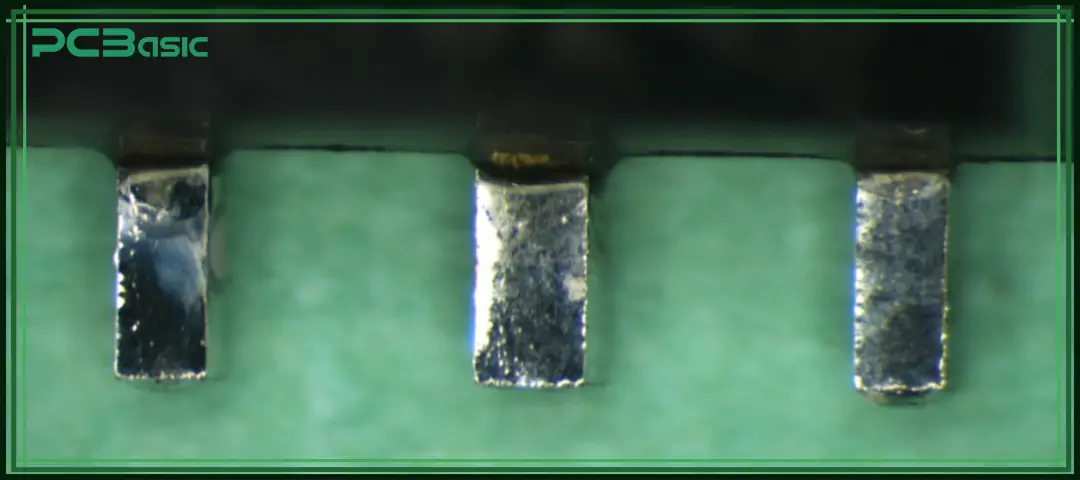
In solderability testing, the most common method is the dip-and-look test. The process is very simple: First, apply flux to the leads or the PCB pads, then immerse them in the molten solder for the specified time and depth. Finally, pull them out, and check the coverage of the solder with the naked eye.
According to the J-STD-002 standard, if the solder coverage rate reaches over 95%, it is considered qualified.
If we need more scientific testing data, we will use wetting balance testing, which is also known as the meniscograph testing. This method can record the wetting force generated by the solder on the metal surface over time and produce a wetting curve.
Through this curve, several key indicators can be obtained:
• Time to Wetting, T₀ —— the time required for the surface to be wetted by solder;
• Maximum Wetting Force, Fmax —— the maximum attractive force when solder adheres to the metal surface;
• Rate of Wetting— the speed at which solder spreads.
These data can help manufacturers compare the effects of different surface treatments, identify potential surface defects, and ensure compliance with the requirements of J-STD-002 and J-STD-003. Because the wetting balance testing provides quantitative results, it is regarded as one of the most advanced and reliable methods for solderability testing at present.
With the popularity of surface-mount technology (SMT), another method has also been widely used, that is, surface-mount simulation. This method is not merely tin immersion but rather tests through a process that is closer to actual production: first, solder paste is printed on the test board; then, the components are placed onto the board, and finally, the soldering is completed through a reflow oven.
This kind of soldering testing can simulate the actual production environment more realistically, especially suitable for those fine-pitch or leadless devices, such as BGA, QFN, etc.
|
Method |
Key Features |
Pros |
Cons |
Best Use |
|
Dip-and-Look |
Qualitative, visual check after solder dip |
Fast, low-cost, simple; defined in J-STD-002 |
Subjective, no data |
Basic inspection, quick screening |
|
Wetting Balance |
Quantitative measures wetting force vs. time |
Objective data (T₀, Fmax, rate); meets J-STD-002/003 |
Needs equipment, higher cost |
High-reliability, R&D, surface finish comparison |
|
SMT Simulation |
Simulates real reflow with solder paste |
Closest to real assembly; ideal for BGA, QFN |
Time-consuming, costly |
SMT packages, advanced process validation |
In addition to the common dip-and-look and wetting balance testing, more in-depth analysis is required in some cases. At this point, several advanced methods will be used:
• S-Score Method: Convert the curve obtained from the wetting balance testing into a score and use a number to measure the quality of solderability, facilitating comparisons among different devices.
• High-Magnification Imaging: After the soldering testing is completed, observe the surface of the solder joint under a microscope to determine whether the solder coverage is uniform and if there are any minor defects.
• Re-Tinning and Refurbishment: For components that have been stored for too long or whose solderability has declined due to surface oxidation, the solderability can be restored by re-tinning, making the devices usable again.
• Aging Studies: Before conducting solderability testing, components should first be stored for a long time or undergo steam aging treatment to simulate possible reliability changes during actual use.
These advanced methods enable manufacturers not only to make pass/fail decisions but also to gain a deeper understanding of the performance of components, predict long-term reliability, and enhance the overall quality assurance level.
Overall, solderability testing has become an indispensable part of electronics manufacturing. Whether it is dip-and-look, wetting balance testing or SMT simulation, the aim is to ensure the reliability of solder joints. By leveraging standards such as J-STD-002 and J-STD-003, as well as advanced methods like S-Score and re-tinning, manufacturers can not only control production costs but also enhance long-term reliability, ensuring that every solder joint of electronic products is firm, safe and future-oriented.

Assembly Enquiry
Instant Quote
Phone contact

+86-755-27218592
In addition, we've prepared a Help Center. We recommend checking it before reaching out, as your question and its answer may already be clearly explained there.
Wechat Support

In addition, we've prepared a Help Center. We recommend checking it before reaching out, as your question and its answer may already be clearly explained there.
WhatsApp Support

In addition, we've prepared a Help Center. We recommend checking it before reaching out, as your question and its answer may already be clearly explained there.