Global high-mix volume high-speed PCBA manufacturer
9:00 -18:00, Mon. - Fri. (GMT+8)
9:00 -12:00, Sat. (GMT+8)
(Except Chinese public holidays)
Global high-mix volume high-speed PCBA manufacturer
9:00 -18:00, Mon. - Fri. (GMT+8)
9:00 -12:00, Sat. (GMT+8)
(Except Chinese public holidays)
HomePage > Blog > Knowledge Base > 3 layer PCB: Why It’s Rarely Used and When It Makes Sense
Usually, the number of layers of a circuit board is 2, 4, 6, 8... Different numbers of layers correspond to different design complexities and implementation paths. Among them, 2-layer and 4-layer circuit boards are the most widely used. However, in this article, we will discuss 3 layer circuit boards. 3 layer circuit boards seem to offer a "compromise option", but they are rarely adopted in practical projects.
Next, in this article, we will introduce the 3 layer PCB in detail. We will start from the basic concepts and gradually analyze its layer structure, design logic, and so on. By reading this article, we can have a clearer understanding of the position of the 3 layer PCB in the entire multi-layer PCB system and how to properly view it in engineering design. Without further ado, let's get straight to the point!
According to the common definition in the industry, a PCB with three or more copper layers is generally considered a multilayer PCB. Therefore, from a classification perspective, a 3 layer PCB board falls within the category of multilayer PCBs.
In engineering practice, many designers are not familiar with this type of board. A 3 layer PCB is a multilayer PCB composed of three layers of conductive copper foil laminated with insulating dielectric layers. Unlike traditional 2-layer boards that only have copper layers on the top and bottom surfaces, a 3 layer PCB board has an additional inner copper layer between the two outer copper foil layers.
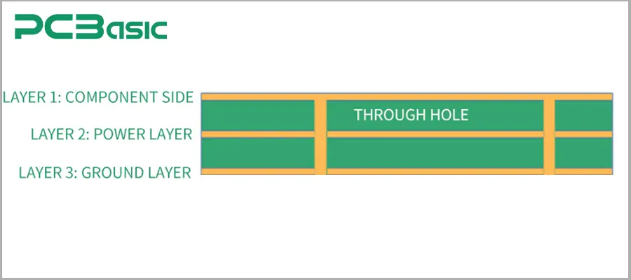
From the perspective of PCB layer structure, a 3 layer PCB typically includes:
The two outer copper layers are typically used for component placement, signal routing, and copper pours, depending on the design requirements.
One inner copper layer is used for signals, power supply or grounding as per design requirements.
As shown in the following figure,
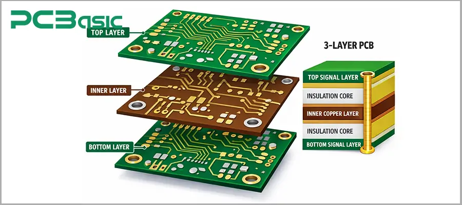
The most notable feature of a 3 layer PCB is its odd-numbered layer structure. This makes it significantly different in structural form from most standard multilayer PCB designs. In conventional multilayer PCB designs, copper layers are typically symmetrically distributed around the centerline of the board thickness, but a 3 layer PCB does not inherently possess this symmetry. This is the reason for its certain special characteristics in design and application.
From a functional perspective, there is no unique or fixed definition for a 3 layer PCB. The specific uses of each layer highly depend on the project requirements and the adopted 3-layer PCB stackup. The flexibility of 3-layer PCBs theoretically offers more design options. Therefore, in some scenarios, 3-layer PCBs seem more attractive than 2-layer boards.
It should be noted that a 3-layer PCB should not be simply regarded as a simplified version of a 4-layer PCB. Although it shares certain similarities in form with other types of PCBs, its electrical characteristics, structural responses, and design constraints are all distinct.
The layered structure of a 3 layer PCB design directly determines the routability of the circuit board, the allocation of layer functions, and the overall design concept. Unlike common 4-layer or 6-layer PCBs, there is no industry-wide "standard stackup" for 3 layer PCBs. The 3 layer PCB stackup needs to be flexibly defined based on the specific project goals.
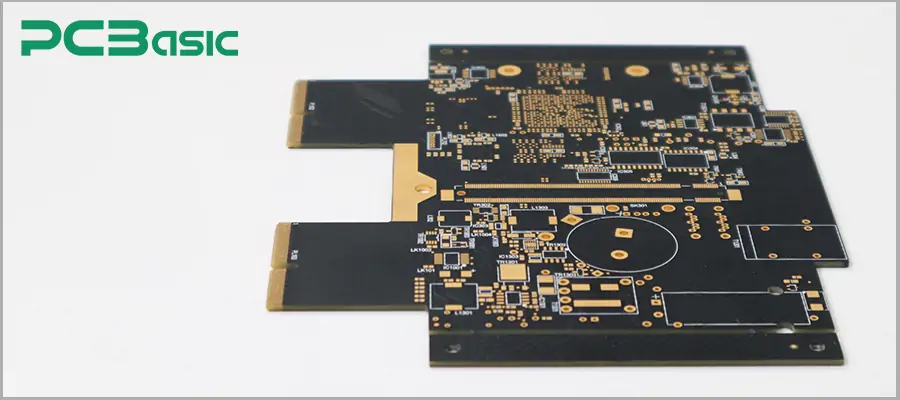
From the basic composition of PCB layers, a 3 layer PCB board is usually composed of two outer layers of copper foil and one inner layer of copper foil. The core difference among different stacking methods lies in the different functional roles of the inner layer copper foil. Here are several typical 3 layer PCB stacking methods:
1. Signal / Ground / Signal
This stacking form is the most easily understandable and frequently discussed structure among 3 layer PCBs:
Top layer: Signal layer
Inner layer: Full surface or large area grounding layer
Bottom layer: Signal layer
In this stackup, the inner copper foil serves as the reference layer, providing a return path for the signals on the outer layer. This stackup is suitable for projects that wish to introduce the basic signal reference concept in a 3 layer PCB design.
2. Signal / Power / Signal
Another common 3 layer PCB laminating method is to use the inner layer as the power distribution layer:
Top layer: Signal layer
Middle layer: Power layer
Bottom layer: Signal layer
The layering concept of this 3 layer PCB board aims to simplify the power wiring, concentrating the power distribution on the inner layer and freeing up the wiring space on the outer layer. This structure requires clear power supply paths but has a relatively simple overall circuit complexity.
3. Signal / Signal / Signal
In some projects, the three layers of copper foil in a 3 layer PCB might all be used for signal routing:
Top layer: Signal
Middle layer: Signal
Bottom layer: Signal
This stackup is rarely recommended in practice and is usually only considered when routing density is the primary constraint. The core objective of this layered structure is simply to increase the number of available wiring layers in order to address the issue of insufficient wiring density.
No matter which of the 3 layer PCB laminated structures is adopted, they all share several common features:
If the number of layers is odd, the structure is naturally asymmetric.
The inner layer functions can be variable, but they must be clearly defined in advance.
The selection of the stack-up is highly related to the design goals of a 3 layer PCB.
Therefore, when planning a 3 layer PCB, it is necessary to independently assess the rationality of the layer function allocation, and one cannot simply apply the common multi-layer PCB design experience.
The 3 layer PCB board is not commonly used. Let's start by discussing the performance of the PCB layers in odd-numbered layers in practical engineering.
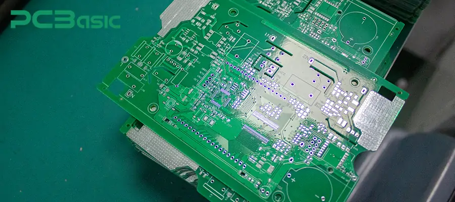
1. The odd-layer structure is not a common feature in multi-layer PCB design.
Most standard multilayer PCBs adopt an even-numbered layer structure, such as 4 layers, 6 layers, or 8 layers. This symmetrical layer structure is more conducive to controlling the board thickness, the lamination process, and the distribution of copper layers. While the 3 layer PCB stackup design (3 layer PCB stack) is of an odd-numbered layer structure, which by itself does not conform to the conventional "paired layer" design concept.
This means that during the design and manufacturing process, many default assumptions – including material configuration, dielectric thickness planning, and process parameter settings – cannot be directly applied to a 3-layer PCB. This "non-standard nature" increases the uncertainty in communication and execution between the design and manufacturing processes.
2. The 3-layer PCB is more difficult to achieve structural balance.
Typically, multi-layer PCBs maintain structural balance by symmetrically distributing copper layers and dielectric layers, ensuring the stability of the circuit board during heating and pressure applications. However, for a 3-layer PCB, since the number of layers is odd, there is a tendency for the copper distribution on the outer and inner layers to become unbalanced.
This imbalance is magnified during processes such as lamination, soldering, and reflow soldering, thereby affecting the flatness of the board. The flatness then relates to the assembly yield, connector assembly, structural assembly, and long-term reliability. This is one of the reasons why 3-layer PCBs are rarely used.
3. Compared with the 4-layer PCB, the cost advantage is not significant.
In many cases, the cost of a 3-layer PCB is close to that of a standard 4-layer PCB, and may even be higher due to non-standard process setup.
The 3-layer PCB also requires multi-layer board lamination process and strict process control. Moreover, in most factories, the 3-layer PCB board is more similar to the 4-layer board in terms of process complexity and production preparation. When the cost is similar but the performance improvement is limited, the 3-layer PCB is not cost-effective.
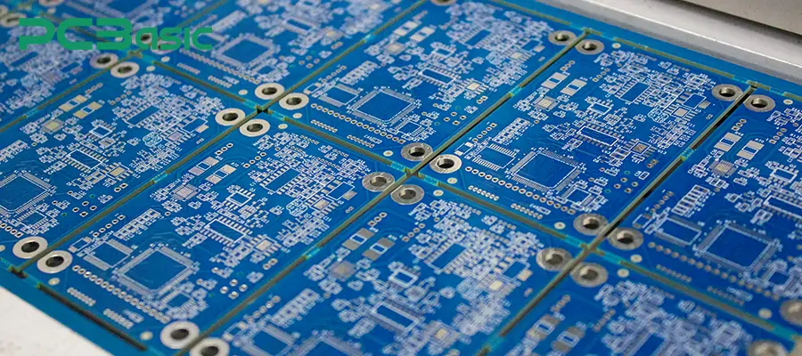
4. Electrical performance is not always "in the middle"
Many people intuitively believe that the electrical performance of a 3-layer PCB stack-up structure should be between that of a 2-layer board and a 4-layer board. However, in practical applications, this "middle state" is not stable.
In standard multilayer PCB design, one of the core significances of increasing the number of layers is to establish stable and continuous reference layers and return paths. In a 3-layer PCB, usually only one inner layer can be used as a reference layer, while the remaining outer layers still undertake a large amount of wiring tasks. This makes it easier for signals to be affected by changes in reference conditions when crossing layers or passing through partitioned areas.
5. Common outcomes in actual engineering decisions
If the circuit is simple and cost-oriented, a 2-layer PCB is more direct and economical. If better electromagnetic control or a more stable structure is required, a 4-layer multilayer PCB better meets engineering expectations. Therefore, among the common types of PCBs, 3-layer PCB boards are more often chosen as a specific scenario option rather than the mainstream solution.
The 3-layer PCB has its advantages and disadvantages. Now, let's take a look at them together.
|
Advantage Area |
Description |
|
Layer count |
More pcb layers than a 2-layer board, providing additional routing resources |
|
Routing flexibility |
Extra internal layer helps relieve routing congestion in moderate designs |
|
Functional allocation |
Internal layer can be assigned as power, ground, or signal depending on the 3-layer PCB stackup |
|
Multilayer structure |
Qualifies as a multilayer PCB, enabling inner-layer processing |
|
Design scenarios |
Suitable for constrained or legacy 3-layer PCB board applications |
|
Limitation Area |
Description |
|
Structural symmetry |
Odd number of pcb layers makes natural layer balance harder to achieve |
|
Reference planes |
Only one internal plane limits flexibility in multilayer PCB design |
|
Stackup standardization |
Fewer widely accepted 3-layer PCB stackup standards |
|
Electrical predictability |
Signal behavior more sensitive to layout decisions |
|
Cost efficiency |
Manufacturing complexity close to standard multilayer PCB boards |
|
Scalability |
Harder to reuse across product families compared to common types of PCB |
In certain specific applications, we may explicitly need to adopt a 3-layer PCB. How can we design and manufacture a 3-layer PCB properly? The following suggestions from several aspects are for your reference.
1. Layer planning and layer function allocation
Since there are only 3-PCB layers, the functions of each layer need to be planned out clearly in advance.
Common layer allocation methods include:
Top layer: Signals and components
Inner layer: Power layer, ground layer, or mixed-signal layer
Bottom layer: Signals and components
Unlike typical multi-layer PCB designs, 3-layer PCBs usually have only one internal reference layer. This means:
Power and ground often need to share the same inner layer, or be achieved through partitioning
The continuity of the reference for high-speed signals is more difficult to guarantee
The selection of the layer stack directly affects EMI, impedance control, and signal integrity
Therefore, the layer structure must be determined early in the design process. Otherwise, if modifications are needed later, the cost will be higher and the risks will be greater.
2. Symmetry of Structure and Warpage Control
The 3 layer PCB is inherently a non-symmetric structure. This can lead to some practical problems:
The copper distribution on the upper and lower layers is uneven, which may cause warping during the pressing and reflow soldering processes.
The thickness of the dielectric layers on the inner layer is different, increasing the internal stress of the board.
The stability requirements for panel handling and reflow process are higher.
To reduce risks, the following are usually required during manufacturing:
Try to balance the distribution of copper sheets at the top and bottom
Strictly control the thickness of the medium
Adjust the lamination parameters according to the 3 layer structure
These additional controls make the manufacturing complexity of the 3 layer PCB board much higher than that of the ordinary double-layer board.
3. Signal Integrity and Reference Layer Management
In many 3-layer PCB designs, there is only one primary reference plane, which places higher demands on return path planning.
Common design principles include:
Place critical high-speed signals as close as possible to the inner reference plane.
Avoid splitting the reference layer beneath critical signal paths.
Reduce unnecessary through-hole jumps and prevent the interruption of the return path.
4. Power Distribution and Power Supply Strategy
In a 3 layer PCB, power distribution is also a matter that requires careful consideration.
Common solutions include:
Making the inner layer a complete layer, with the power supply on the outer layer achieved through copper sheets or traces.
Dividing the inner layer into power zones and areas.
Using large areas of power copper sheets on the signal layer.
Compared to a standard 4-layer PCB, these solutions typically have less margin in terms of noise control and power integrity. Therefore, they need to be fully evaluated during the design stage.
5. Manufacturing Process and Cost Characteristics
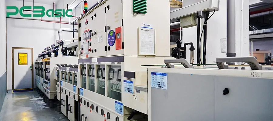
Although the number of PCB layers in a 3-layer board is less than that of a conventional multilayer board, the manufacturing process still requires:
Inner layer imaging and etching
Multilayer lamination process
Multilayer alignment and registration control
In actual production, the process flow of a 3-layer PCB is more similar to that of a multilayer PCB. Therefore:
Compared with a 4-layer board, the cost advantage is not obvious
The delivery time may not be shorter
The yield risk is higher, which requires stricter design rules and more rigorous DFM control.
6. Design Reusability and Subsequent Scalability
From the perspective of the product lifecycle, the scalability of a 3-layer PCB board is relatively limited:
When upgrading to a higher number of layers, re-design is often required.
The stack-up and design rules are not easily reusable across different projects.
The available suppliers and mature processes are relatively limited.
For one-time projects or existing systems, such a structure is acceptable. However, if the product is planned for long-term iteration or platform-based development, a careful assessment of whether a 3-layer PCB is suitable is necessary.
A 3-layer PCB is a multi-layer PCB structure with a specific application scenario. It is not a universal solution. In terms of wiring resources and functional allocation, a 3-layer PCB outperforms a 2 layer PCB. However, in terms of structural symmetry, electrical stability, and manufacturing complexity, a 3-layer PCB does not have significant advantages.
Time is money in your projects – and PCBasic gets it. PCBasic is a PCB assembly company that delivers fast, flawless results every time. Our comprehensive PCB assembly services include expert engineering support at every step, ensuring top quality in every board. As a leading PCB assembly manufacturer, we provide a one-stop solution that streamlines your supply chain. Partner with our advanced PCB prototype factory for quick turnarounds and superior results you can trust.

Assembly Enquiry
Instant Quote
Phone contact

+86-755-27218592
In addition, we've prepared a Help Center. We recommend checking it before reaching out, as your question and its answer may already be clearly explained there.
Wechat Support

In addition, we've prepared a Help Center. We recommend checking it before reaching out, as your question and its answer may already be clearly explained there.
WhatsApp Support

In addition, we've prepared a Help Center. We recommend checking it before reaching out, as your question and its answer may already be clearly explained there.