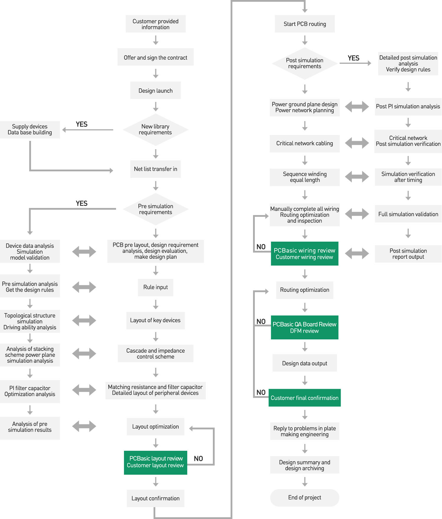
At PCBasic, we strive to lead our customers through the easier and faster PCB development process and fabrication. Our PCB design process includes multiple PCB design steps, including PCB layout steps, PCB routing process, PCB design and manufacturing, SMT stencil design, and flow of complete PCB design.
We also offer our customers a variety of pre-fabrication steps, including PCB design process steps such as PCB design procedure, PCB layout design, and producing a clear plan and definition for PCB design flow.
The first step in PCB design will always be an ideal stage, and we take our customers from that stage to prototyping to full-scale manufacturing. Using our proven PCB design process, we can ensure top quality each time. Our years of experience in developing a custom PCB design process for our customers at scale has proven itself each time.
The first step in PCB design starts here, with PCBasic.
We use cookies to enhance your experience, analyze traffic, and provide personalized content. By clicking “Accept Cookies”, you agree to our Cookie and Privacy Policy.
Manage Cookie Preferences
We use cookies to enhance your browsing experience. Please review the details of each cookie category below and choose your preferences.
Strictly Necessary Cookies
These cookies are essential for the website to function properly and cannot be disabled. They are typically set in response to actions you take, such as logging in or adding items to your shopping cart.
Performance Cookies
These cookies help us understand how visitors interact with our website by collecting information about traffic and usage. This allows us to measure and improve the website’s performance.
Targeting/Advertising Cookies
These cookies are used to deliver
advertisements relevant to you and your interests. They may also limit the number of times you see an
advertisement and help measure the effectiveness of advertising campaigns.
In addition, we've prepared a Help Center.
We recommend checking it before reaching out, as your question and its
answer may already be clearly explained there.
✖
Wechat Support
In addition, we've prepared a Help Center.
We recommend checking it before reaching out, as your question and its
answer may already be clearly explained there.
✖
WhatsApp Support
In addition, we've prepared a Help Center.
We recommend checking it before reaching out, as your question and its
answer may already be clearly explained there.