RF PCBs: Your Ultimate
Guide to Radio Frequency PCBs
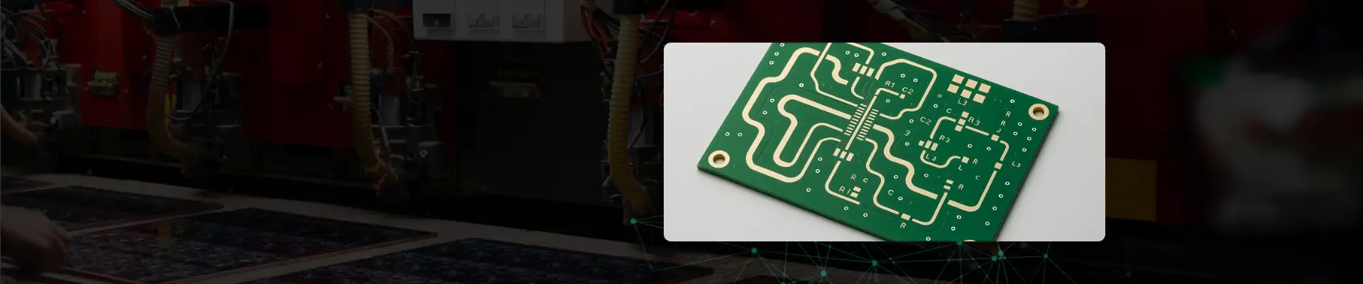
RF PCBs or radio frequency printed
circuit boards are among the fastest-growing areas in PCB manufacturing. They
function with high-frequency signals, especially those in the RF (radio
frequency) range.
It is important to handle the layout
and routing carefully to prevent issues related to signal integrity. This is
because RF PCB layouts could contain digital components and, with careful
layout, could prevent possible interference between the digital & RF
signals.
This article explains what RF PCB is,
its design principles, material considerations, and its layout design. We will
also discuss the common challenges faced during RF PCB design and give possible
tips and solutions. Lastly, we will provide tips and factors to consider before
selecting the best RF PCB manufacturer. Please stay on this page as we explain
the topic further.
What is an RF PCB?
RF describes any frequency where the
emissions of radio waves occur. The RF frequency range usually falls within 300
KHz and 300GHz. The major difference between a microwave PCB and an RF PCB is
the radio frequency they operate on.
An RF PCB is a high-frequency PCB that
functions above 100 MHz, while PCBs operating at frequencies higher than 2GHz
are categorized as microwave PCBs. Both microwave PCBs and RF PCBs are
essential for communication signals in applications requiring the transmission
and receiving of radio signals i.e. radar installations.
RF PCB uses materials with high
thermal conductivity and low dielectric loss. To maintain their signal
integrity, they work with structures of transmission lines and controlled
impedance. Furthermore, RF PCBs have shielding features that help to reduce EMI
(electromagnetic interference). This feature also ensures better signal
transmission.
The applications of RF circuit boards
are diverse. These include radar systems, microwave equipment, and wire
communication systems. Also, these PCBs help to reduce possible issues such as
signal interference, signal loss, and noise. The problems can reduce the
functionality of these high-frequency circuits.
The primary function of a conventional
PCB is to offer electrical connections and mechanical support by mounting
electrical components like capacitors, resistors, and integrated circuits on
its surface and interconnecting them utilizing copper traces.
In contrast, RF circuit boards can
handle radio-frequency and high-frequency signals. Compared to conventional
PCBs, RF PCBs feature unique design requirements and characteristics that allow
effective transmission of signals within a high-frequency range.
RF PCB Applications and Material Matching
Guide
RF Application
RF Materials
Bonding Materials
Attributes
Military & Space Application
RO4000
RT/Duroid
RO4450F
RO4450B
The most effective in thermal and electrical
performance as well as environmental durability
Consumer Electronics
RO4835
RO3010
RO3006
2929 Bondply
Bondply
RO3000 Series
It is profitable and has reliable thermal and
electrical features
Medical
RO4350B
2929 Bondply
RO4400 Bondply
High-performance features that suit different devices
Industrial
RO4350B
RO4835
XT/Duroid
RO4400 Bondply
2929 Bondply
Great durability as well as environmental resistance
Automotive
RO4000
RO3003
RO4350B
RO4400 Bondply
Great electrical performance that suits standard
manufacturing processes
Higher Power Applications
XT/Duroid
6035 HTC
Not typically required or custom thermal
Excellent thermal management
Core RF PCB Design Guidelines
It is essential to reduce noise,
signal loss, and electromagnetic interference (EMI) during RF PCB design. It is
also essential to maximize signal stability, strength, and bandwidth. Here are
the main design principles for RF PCBs.
Design
Requirements
Before you begin with the RF PCB
design, it is crucial to determine the PCB’s impedance matching, power level,
and frequency range requirements. Also, know the electronic components used
during the PCBA (PCB Assembly).
PCB
Layout
Placing the RF PCB components should
help reduce the length of the signal wire. It should also make use of a few
vias.
In addition, attach smaller components
to critical parts. Remember that the RF lines should be short. This prevents
routing them close to high-speed power planes, digital traces, and other noise
sources.
Grounding
There should be a solid ground plane
beneath the RF traces, to reduce return paths, radiation, and crosstalk.
Impedance
Matching
It is vital to use microstrip
transmission lines. This ensures proper matching of the RF traces’ impedance to
those of the connectors and components. Also, ensure the trace space and width
meet the required tolerances and impedance value.
Shielding
Utilize RF shields or shielded
connectors to avoid possible interference from other sources and RF signal
leakage.
Test
After completing the layout, it is
essential to test the circuit to evaluate its performance. Use an oscilloscope
or network analyzer to measure the bandwidth, return loss, and insertion loss.
Optimization
Make adjustments to the design to
optimize its performance. This is possible by adjusting the trace space, width,
and length. Also, analyze the circuits’ RF behavior using electromagnetic
solution tools.
Generally, RF PCB design requires
proper and meticulous planning. It also requires a vast knowledge of the
principles of RF design. It is possible to create high-performance RF circuits
by following these design guidelines and working with the appropriate
techniques and tools.
About PCBasic
Time is money in your projects – and PCBasic gets it. PCBasic is a PCB assembly company that delivers fast, flawless results every time. Our comprehensive PCB assembly services include expert engineering support at every step, ensuring top quality in every board. As a leading PCB assembly manufacturer, we provide a one-stop solution that streamlines your supply chain. Partner with our advanced PCB prototype factory for quick turnarounds and superior results you can trust.
RF PCB Material Considerations
Below are some material considerations
when manufacturing RF circuit boards.
Dielectric
Constant
The dielectric constant describes the
medium’s electrical signal propagation speed. This speed is inversely related
to the square root of the dielectric constant. Lower values of the dielectric
constant mean faster signal transmissions.
Furthermore, measuring this property
isn’t an easy task. It isn’t just related to the medium’s characteristics but
is closely related to the material’s state during and before the test, the test
frequency, and the test method.
Also, a change in temperature affects
a change in the dielectric constant. This is why you must consider the
temperature while developing some materials. Another factor that affects the
dielectric constant is humidity. This is because water’s dielectric constant
value is 70. Just a small quantity of water will lead to significant changes.
The best material for high-frequency
and high-speed applications is an air medium with copper foil wrapping. Also,
aside from affecting the signal’s transmission speed directly, the dielectric
constant helps to some extent in determining the impedance. In several parts,
this impedance plays a significant role in microwave communication.
Since the dielectric constant usually
changes with temperature change, the microwave materials are traditionally
outdoors, even in space environments.
Loss
Tangent
Loss tangent is another factor that
affects an rf pcb material’s electrical properties. Other names for loss
tangent are loss factor and dielectric loss. This indicates a signal or energy
loss in a medium. This is because whenever high-frequency signals pass through
a medium, molecules in that medium adjust or adapt themselves to conform to the
electromagnetic signals.
However, the molecules are
cross-linked, which makes it almost impossible to adjust itself to, but with
frequency changes, the scorers will continue to move, generate more heat, and
lead to energy loss.
Furthermore, some materials like PTFE
are usually nonpolar. This means an electromagnetic field does not affect them
and, therefore, experiences minimal loss. Also, the loss tangent relates to the
test method and frequency.
Here, there is a general rule – higher
frequencies result in more significant losses. A good example here is
electrical energy consumption. When there is a slight loss in the circuit
design, there can be a massive increase in the battery life. When an antenna
receives the signal, it becomes more sensitive to material loss, and there will
be a clearer signal.
Coefficient
of Thermal Expansion
Denoted as CTE, it indicates how a
material contracts and expands when subjected to different temperatures. In
addition, it is an essential criterion when choosing materials during
fabrication.
Electrical
Strength
Electrical strength has a close
relationship with the dielectric strength of a material to be utilized in a
circuit. When working with low-power boards, this factor may not be
significant. However, for high-power applications such as RF PCBs, electrical strength
is very essential.
Thermal
coefficient
It is crucial to consider the
material’s thermal coefficient before you choose. In some cases, little changes
in the value of the thermal coefficient will cause a shift in frequency
responses. Because RF PCBs are usually exposed to fluctuating temperatures, it
is advisable to use materials with a thermal coefficient value below 50 ppm/°C.
Glass
Transition Temperature
Denoted as Tg, it is the temperature
at which a PCB substrate can change from its glass state to a softened one,
which could easily be deformed. After the material cools down, it returns to
its former state.
Moisture
Absorption
A material’s moisture absorption is
its ability to restrict water absorption, most especially when inserted in
water. Usually, moisture absorption affects a material’s electrical and thermal
properties. Make sure you understand whatever environment the board will work
on.
Decomposition
Temperature
The decomposition temperature, denoted
as Td, signifies the temperature whereby an RF PCB material undergoes
mechanical decomposition. Make sure that the materials utilized will sustain
whatever temperature the board will have to operate under. This is necessary
because immediately after a material reaches its decomposition temperature, it
is irreversible.
RF PCB Layout and Component Placement
RF circuit boards are usually more
sensitive to interference. This is why RF PCB designs require tighter
tolerances. Specifically, reflections, ringing, and noise have to be accounted
for. This requires handling the impedance matching with care during routing.
Furthermore, signal return paths are
essential in an RF design's high-frequency circuits. These signal return
currents follow the route of the lowest impedances. During the RF PCB layout
process, circuit simulation becomes important to discover problem areas and
find solutions.
There are deviations to the
traditional PCB layout rules which should deliver the most appropriate signal
performance. These include smaller pad sizes and tight placement clearances.
However, it would help if these modifications were made when necessary to
maintain the required DFM rules to ensure error-free assembly and fabrication.
Let's consider some of the
requirements to achieve the best performance.
RF
Component Placement
During RF circuit block component
placement, the circuitry usually requires a tighter & firmer part
placement. Modifying this component placement is one compromise the designer
has to manage carefully to be sure you can achieve the board creation with
standard and automated equipment for assembly. This helps to prevent the
escalation of manufacturing costs.
Furthermore, an RF board usually has
extra metal on its external layers for use by its power networks, while
components are typically placed in those areas. Although this connection might
work great for the RF circuitry’s performance, PCB assembly issues may arise.
Also, during layout, you may need to
alter the components. These could include changing the PCB footprint pads'
shape and size and incorporating metal shapes and features in the footprint.
These tasks are handled individually by the board's components rather than
altering the base library section. Now, let's consider some trace routing
requirements that may come into play during RF PCB design.
Trace
Routing
Like all high-speed routings, direct,
short routing with different widths will be necessary for higher current power
traces and controlled impedance routing. Below are some points on RF routing to
consider.
● The majority of
trace routing has to be added manually for some RF topologies
● Setting up and
utilizing the design rules is vital for success
● Also, routing
features like copy and paste could be important when replicating similar
circuitry areas
● Vias provide
fencing around the ground plane areas for shielding
● Mitered corners
help to reduce any impedance fluctuation
For several RF designs, some routing
areas are treated as components. Routing of this type requires tools that
accommodate parametric component routing to send the trace segments into the RF
analysis systems.
Furthermore, ground and power planes
require higher power in RF designs and ensure thermal reliefs handle the
current during automated soldering. Also, it is essential to create metal areas
that are oddly shaped for RF elements, utilizing your CAD tools’ drafting
capabilities and then converting these areas to intelligent net objects.
Common Challenges and Solutions During RF
PCB Design
Common challenges in RF PCBs include
minimizing weight, outgassing, bleeding prevention, and impedance matching.
Below are some other challenges:
Difficult
design process
For multiple-layer satellite PCBs, you
must keep different components separately. This decreases possible issues
during the assembly process. Furthermore, RF PCBs require many layers, with the
top layer featuring RF signal lines and a power stage. Also, the board requires
ground layers underneath components that have RF signals.
Noise
RF signals are susceptible to noise
and even more sensitive to different noise types than standard PCBs.The4e are
different noise types, including band limited, pink, or white and shot,
thermal, flicker, phase, and avalanche noise. Reducing the signal noise,
reflection, and ringing to a feasible extent is important.
Wide
Range of Temperature
A change in temperature level is
another common challenge to consider. Changing a satellite's temperature could
alter the material features of the PCB. Checking the temperature coefficient is
necessary for comparing board materials and their suitability for various
satellite applications.
Furthermore, RF PCBs must have the
ability to dissipate heat properly, most especially in small and constricted
areas. Look into the thermal conductivity of the PCB to understand the manner
of how the RF PCB material dissipates heat.
Reliability
Reducing weight concerns the
increasing use of multilayer circuit boards and increased RF circuitry density.
Furthermore, the plated through holes reliability for interconnections between
the layers has become a concern when operating in extreme temperatures in
space.
What is a Microwave PCB?
The microwave PCB is a kind of RF
PCB. It is specially designed for high-frequency signal transmission. Its
operating frequency is usually higher than 1 GHz; that is, it enters the
"microwave" frequency band. Simply put, if your circuit needs to
transmit signals at very high frequencies, such as in satellite communications,
5G base stations, high-speed radars, or military radar systems, then you are
likely to be using a microwave PCB.
RF vs. Microwave PCBs
Although all microwave PCBs
belong to RF circuit boards, that is to say, they are all used in applications
within the radio frequency range, not every RF PCB is competent for signal
transmission at the microwave level. For instance, some RF PCBs with operating
frequencies ranging from 100 MHz to 1 GHz, although also used in scenarios such
as wireless communication and Bluetooth, cannot meet the higher requirements of
microwave systems for accuracy, impedance control, and material stability.
Therefore, when conducting RF PCB
design, especially when it comes to the microwave frequency band, the
appropriate RF PCB materials must be selected from the very beginning, and
strict RF layout and RF PCB design guidelines must be followed. This can not
only ensure the transmission quality of the signal, but also significantly
improve the overall reliability of the product.
Here we go through the
differences between RF PCBs and microwave PCBs in a table:
Feature
RF PCB (Radio Frequency PCB)
Microwave PCB
Frequency Range
100 MHz – 1 GHz (typical RF
range)
1 GHz and above (microwave
range, commonly used in 3–30 GHz applications)
Signal Type
Low to mid-frequency RF signals
such as FM, Wi-Fi, Bluetooth, Zigbee
High-speed, high-frequency
signals such as radar waves, millimeter-wave communication, satellite links
Low Dk (≈ 2.2–3.0), extremely
low Df (≈ 0.0009–0.003) for minimal signal loss
Layer Structure
Can be 2-layer or multilayer;
suitable for general RF PCB design
Typically multilayer with
stringent RF layout and isolation control
Application Scenarios
Wireless modules, Bluetooth
devices, RF remotes, RF transceivers
Satellite systems, 5G mmWave
modules, military radar, aerospace communication systems
Design Complexity
Relatively moderate, with
standard RF PCB design guidelines
High complexity, requiring
strict RF layout guidelines and microwave impedance matching
Cost and Manufacturing
Standard PCB processes,
moderate cost
Complex fabrication, tight
tolerance, higher cost due to material and performance requirements
Understanding these differences
helps engineers and designers select the appropriate RF PCB material and board
type for their specific frequency range and application. Choosing between a
general RF circuit board and a high-performance microwave PCB is critical to
ensuring signal quality and overall system reliability.
Choosing a Reliable RF PCB Manufacturer
Before you choose an RF PCB
manufacturer, there are some features to consider
Experience
You wouldn’t want to work with a
company without experience in RF PCB manufacturing. Perfection usually comes
when there is experience. Experienced manufacturers use recent technologies and
machinery during high-frequency PCB manufacturing.
With experience, the chances of the RF
PCB failing are low. To achieve the best results, hire a manufacturer that has
vast experience in the field.
Certification
Quality should be a crucial factor
before choosing an RF PCB manufacturer. The first thing to consider is the
manufacturer’s quality management system (QMS). The minimum requirement is the
ISO 9001 certification. It indicates the presence of a basic QMS.
Included are work instructions,
procedures, processes, quality manuals, quality policies, preventive actions,
etc. Some certifications help to prove a company’s competence. These include
ISO 13485, A-610, A-600, and IPC J-STD.
Technical
Capabilities
It is vital to work with an RF PCB
manufacturer with outstanding technical capabilities like PCBasic. These
capabilities include appropriate designs and material selection, processing
technology, strict quality control, and condition of equipment used.
Fair
Pricing
Before you work with an RF PCB
manufacturer, know the cost. You can achieve this by checking out the websites
of different manufacturers to understand the different market prices.
Conclusion
The design and manufacturing of RF
PCBs require the appropriate material selection, design rules, and
manufacturing processes. This is why it is important to work with a reliable RF
PCB manufacturer like PCBasic.
We use cookies to enhance your experience, analyze traffic, and provide personalized content. By clicking “Accept Cookies”, you agree to our Cookie and Privacy Policy.
Manage Cookie Preferences
We use cookies to enhance your browsing experience. Please review the details of each cookie category below and choose your preferences.
Strictly Necessary Cookies
These cookies are essential for the website to function properly and cannot be disabled. They are typically set in response to actions you take, such as logging in or adding items to your shopping cart.
Performance Cookies
These cookies help us understand how visitors interact with our website by collecting information about traffic and usage. This allows us to measure and improve the website’s performance.
Targeting/Advertising Cookies
These cookies are used to deliver
advertisements relevant to you and your interests. They may also limit the number of times you see an
advertisement and help measure the effectiveness of advertising campaigns.
In addition, we've prepared a Help Center.
We recommend checking it before reaching out, as your question and its
answer may already be clearly explained there.
✖
Wechat Support
In addition, we've prepared a Help Center.
We recommend checking it before reaching out, as your question and its
answer may already be clearly explained there.
✖
WhatsApp Support
In addition, we've prepared a Help Center.
We recommend checking it before reaching out, as your question and its
answer may already be clearly explained there.


 About PCBasic


