Why do people working on the circuit board production line all wear a wristband? This is related to the hazards of electrostatic discharge (ESD). You may not have a specific concept of the dangers of electrostatic discharge. Electrostatic discharge is a very common yet often underestimated threat. It can instantly damage sensitive semiconductor devices, even in highly controlled production environments.
If technicians do not wear the appropriate anti-static protection equipment when touching the printed circuit board, the electrostatic discharge may already have occurred at the moment their fingers touch the pads. It may have damaged the microcontroller on the board, or left a hidden hazard inside the chip that will only become apparent in the future. In summary, electrostatic discharge cannot be ignored, and effective electrostatic discharge protection is extremely important. Next, this article will delve into the knowledge related to ESD protection. First, let's start with the concept of electrostatic discharge.
Understanding Electrostatic Discharge (ESD)

Electrostatic discharge is abbreviated as ESD. It refers to the phenomenon where an electric current suddenly flows between two objects with different potentials. This discharge can occur either through direct contact or due to the breakdown of the surrounding medium (such as air). There are many occurrences of electrostatic discharge in daily life, such as the crackling sound when taking off a sweater in winter, and the tiny sparks that flash at the plug when unplugging the charging cable. This phenomenon has almost no impact on the human body, but in electronic manufacturing, it poses a much greater threat to PCB and PCBA.
Principles of ESD
The principles of ESD mainly consist of three aspects: the generation and accumulation of static charges; the discharge process of static electricity in the electronic manufacturing environment; and how these discharges interact with circuits and cause ESD damage. So how are static charges generated and accumulated? There are various mechanisms for the generation of static charges, among which the most common ones are:
Electrostatic charging by friction - When two materials rub against each other, electrons will transfer and form charges on the surface.
Contact separation - For example, when plugging in or unplugging connectors, the surface charges will redistribute and accumulate.

Inductive charging - When close to an electrified body, the surface of a conductor will induce opposite charges, thereby creating a potential discharge risk.
Under certain conditions, these static charges will be released rapidly, resulting in an electrostatic discharge. This discharge phenomenon is particularly dangerous in electronic manufacturing because it can occur within milliseconds or even nanoseconds and directly enter the circuit through various paths. For instance, there are cases where the operator's finger jumps directly to the pad or pin; the ungrounded soldering iron tip conducts to the component; and discharge occurs between two closely placed or touching connectors. These instantaneous pulses can reach up to several thousand volts, and their peak current is sufficient to damage the internal structure of the component within nanoseconds.
Then, when the high-voltage pulse enters the electronic circuit, it will trigger the following damage modes:
Semiconductor breakdown - High voltage directly penetrates the MOSFET, diode, or the junction area within an IC.
Metal traces melting - Instantaneous high heat generated by a pulse current melts the fine copper wires on the PCB.
Insulation breakdown - The dielectric of a capacitor or the PCB insulation layer is penetrated by high voltage, resulting in leakage or short circuit.
Some damages occur immediately, while others are latent defects. These latent defects do not manifest during the factory inspection, but gradually worsen over time during use.

What is ESD Protection?
ESD protection is a comprehensive system consisting of design strategies, protective devices, and production control measures. Its purpose is to prevent or reduce failures caused by electrostatic discharge.
Circuit-level protection is usually achieved by adding ESD protection devices around sensitive components. For example, varistors and RC filters are used to absorb surges and suppress high-frequency noise.
There is also manufacturing-level protection. This level of protection includes:
ESD protection equipment: antistatic wrist straps, antistatic floor mats, grounding workbenches, ion blowers;

ESD protection methods: personnel grounding, tool grounding, material antistatic treatment, environmental humidity control;
ESD protection techniques: including static power source identification, ESD risk assessment, real-time monitoring systems, etc.
If there is no effective electrostatic discharge protection, immediate catastrophic failures may occur. For example, during PCB assembly soldering, a single uncontrolled discharge can destroy an IC or MOSFET.
Importance of ESD Protection in PCB
ESD protection is very important for PCBs and PCBAs. For instance, in a USB product without any protective design, failure of the USB interface is a very common malfunction. This is because when plugging or unplugging the data cable, static electricity will be released through the metal casing or signal pins, directly damaging the USB transceiver chip. Besides, there is also a very common problem of HDMI receiver damage. ESD events occur frequently, and ESD protection is very necessary.
Furthermore, the industry has a set of minimum protection standards. These standards require that the equipment should still function properly under the most stringent Level 4 testing conditions. The standards also specify the factory-level ESD control procedures, including ESD protection methods, personnel grounding, workbench grounding, antistatic packaging and other measures. This means that during the production process, these standards need to be followed to ensure the long-term reliability in real-world applications.

ESD Protection Standards
As mentioned earlier, there is a set of protection standards within the industry. Now, let's introduce these standards. These standards not only provide guidance for PCB design and manufacturing practices, but also establish a unified framework for evaluating ESD protection methods (ESD protection methods) and compliance requirements.
IEC 61000-4-2 is one of the most widely adopted standards for evaluating the electrostatic discharge immunity of equipment. It clearly stipulates the test levels, discharge methods, and the performance evaluation criteria for the equipment under ESD shock.
Its test level is:
|
Level
|
Contact Discharge Voltage
|
Air Discharge Voltage
|
Typical Environment
|
|
Level 1
|
±2 kV
|
±2 kV
|
Low-static environments, such as laboratories
|
|
Level 2
|
±4 kV
|
±4 kV
|
Offices or light industrial environments
|
|
Level 3
|
±6 kV
|
±8 kV
|
General industrial environments
|
|
Level 4
|
±8 kV
|
±15 kV
|
High static-risk areas (dry climates, outdoor equipment, etc.)
|
In the IEC 61000-4-2 test, the equipment must continue to operate normally after an ESD event, without any permanent damage or data loss. Short-term performance fluctuations (such as display flickering) are acceptable, but any functional degradation or irreversible ESD damage is regarded as a failure.
This standard requires industrial-grade PCB and PCBA products to meet the Level 4 design goals. In such cases, designers typically:
Add low-capacitance ESD protection devices at high-speed ports such as USB, HDMI, and Ethernet;
Use short and direct grounding paths in ESD protection circuits to reduce inductance;
Combine shielding, grounding planes, and optimized routing in the layout design as part of the ESD protection types.
Other Industry Standard
In addition to the requirements of IEC, there are two key standards that play a significant role in the ESD protection strategies of the electronics manufacturing industry. They are ANSI/ESD S20.20 and the JEDEC ESD device classification standard.
|
Standard
|
Scope
|
Key Applications
|
|
ANSI/ESD S20.20
|
Specifies factory-level ESD protection methods, including personnel grounding, workstation grounding, ionization, humidity control, and antistatic packaging
|
PCB assembly lines, electronic manufacturing facilities
|
|
JEDEC ESD Device Classification
|
Classifies devices based on ESD damage tolerance using HBM (Human Body Model), MM (Machine Model), and CDM (Charged Device Model)
|
Component selection, reliability engineering, and setting types of ESD protection in design
|
ESD Protection Methods and Circuit Design
The commonly used ESD protection methods are:
Grounding and Shielding: A stable and low-impedance grounding solution is one of the most effective ESD protection techniques. The ESD current is routed through a low-resistance and low-inductance path, significantly reducing the energy that enters the sensitive circuits. This shielding measure can deflect the electrostatic discharge to a safe path, further protecting the internal components.
PCB-Level ESD Suppression: When designing PCBs, we place dedicated ESD protection devices near the vulnerable input and output ports, such as TVS diodes, voltage-sensitive resistors, or RC filters. This PCB-level ESD suppression method dissipates the ESD before it reaches the core circuit.

System-Level ESD Protection: This method considers the protection of the entire device, including connectors, enclosures, cables, and submodules.
Manufacturing-Level ESD Control: This protection method is mainly aimed at static electricity during production. The control methods include using ESD protection equipment (antistatic wristbands, antistatic leg straps, ion blowers, grounded workbenches, etc.), using antistatic packaging, and controlling the humidity in the workshop.
PCB Layout & Routing Tips
A good PCB layout design and the selection of the appropriate ESD protection devices are equally important. As mentioned earlier, PCB-level ESD protection. Next, we will start from the PCB layout & routing tips and provide practical layout and routing guidelines that can be directly implemented. These guidelines can help ensure that the ESD protection circuits and devices perform at their maximum efficiency in the actual PCB.
1. Reduce the impedance of the ESD path. ESD current flows along the path with the lowest impedance, not necessarily the shortest path. Therefore, during the design and layout process, we should use wider copper wires or ground planes to reduce the resistance and inductance of the grounding path.
2. When laying out, we should make the return path of the ESD current as short and direct as possible because a low-inductance loop can reduce the voltage overshoot during electrostatic discharge.
3. Long PCB traces will act like antennas and absorb and amplify ESD energy. Therefore, we should try to shorten the trace lengths of sensitive signals and ESD protection circuits.
4. Each through-hole will increase inductance and resistance. Therefore, in the ESD protection path, we should avoid using too many through-holes. If necessary, we can use multiple parallel through-holes to reduce the impact.
5. Noise can also be reduced by adding filter components. Ferrite beads, common-mode chokes, and RC filters, etc., can suppress residual ESD energy and prevent high-frequency noise from entering the sensitive areas of the PCB.

ESD Protection in PCBA Manufacturing
It is of great importance to adopt ESD protection methods during the PCB design stage. However, ESD protection should also be considered during the PCB assembly process. This is to prevent the failure of electrostatic discharge protection during assembly and operation. Generally, every PCB manufacturer should implement the following complete ESD protection measures.

Firstly, the construction of an ESD safety workbench is necessary. The ESD safety workbench is the foundation of manufacturing-level ESD control. Each assembly workstation should be equipped with a grounded workbench, an antistatic mat, and a conductive floor connected to the earth. All tools, test fixtures, and welding equipment must also be grounded to provide a safe path for accumulated static electricity. A reasonable workbench layout not only ensures that ESD current is guided to a safe path but also avoids the flow of static electricity through sensitive components.
Secondly, attention should be paid to the storage and packaging of components. Sensitive components should be stored and transported in ESD-safe packaging, such as shielding bags, conductive trays, etc., to prevent ESD damage during internal transportation or shipment. Moreover, the storage area for components should maintain an appropriate humidity level to reduce the accumulation of static charges.
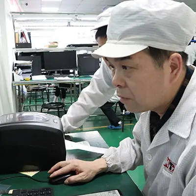
Thirdly, ESD protection equipment should be equipped throughout the production process, including antistatic wristbands, mats, ion fans, etc. These protective devices can prevent ESD damage during manual operations and are very important. Therefore, in addition to having the equipment properly installed, regular testing and maintenance are also required to ensure that they always meet the requirements of ESD protection techniques.

Fourthly, even if the best ESD protection equipment is equipped, improper use will still not be able to effectively protect. Therefore, regular ESD protection training should also be conducted. This will enhance the understanding of all employees about the causes of electrostatic discharge, the existing ESD protection methods, and their responsibilities in the protection process.
Conclusion
ESD protection is no longer an optional feature but a critical requirement that must be strictly implemented. If we can properly plan the ESD protection circuit in the design, follow scientific wiring principles in the PCB layout, and implement rigorous manufacturing-level ESD control during the manufacturing process, then we can significantly reduce the risk of electrostatic discharge damage, ensuring the stable performance and long-term reliability of the product.
 About PCBasic
Time is money in your projects – and PCBasic gets it. PCBasic is a PCB assembly company that delivers fast, flawless results every time. Our comprehensive PCB assembly services include expert engineering support at every step, ensuring top quality in every board. As a leading PCB assembly manufacturer, we provide a one-stop solution that streamlines your supply chain. Partner with our advanced PCB prototype factory for quick turnarounds and superior results you can trust.