Global high-mix volume high-speed PCBA manufacturer
9:00 -18:00, Mon. - Fri. (GMT+8)
9:00 -12:00, Sat. (GMT+8)
(Except Chinese public holidays)
Global high-mix volume high-speed PCBA manufacturer
9:00 -18:00, Mon. - Fri. (GMT+8)
9:00 -12:00, Sat. (GMT+8)
(Except Chinese public holidays)
HomePage > Blog > Knowledge Base > What Is a Gold Plated PCB: ENIG (Immersion Gold) vs. Gold Plated PCB
Surface treatment involves more than just the choice of PCB's appearance. It directly affects the soldering performance, electrical stability, and the long-term reliability of the product. Today, the topic we are going to discuss is one type of surface treatment - gold plated PCB. Among various surface treatment processes, gold plated PCB is widely used in products with high reliability requirements due to its excellent anti-oxidation ability and stable performance.
However, in actual engineering and production communication, the term "gold plated PCB" often leads to misunderstandings. In most cases, it refers to two completely different processes: ENIG (immersion gold plating) and electroplated gold PCB.
Next, in this article, we will introduce gold surface finishes from a manufacturing perspective and systematically compare the differences between ENIG plating and traditional gold plated PCB. First, let's understand what gold plated PCB is.

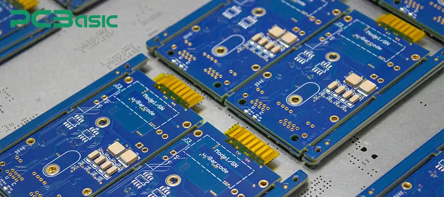
A gold-plated PCB refers to a PCB in which gold is used as the final surface treatment layer on the exposed conductive areas of the board (such as pads, contact points, or connector interfaces). The main purpose of PCB gold plating is to prevent the copper surface from oxidizing and to ensure the stability of electrical connections during assembly and use. In gold-plated circuit boards, the gold layer mainly serves as a surface protection layer.
According to the formation method of the gold layer, gold plated PCBs can generally be divided into two types: immersion gold plating and electroplated gold. We have already mentioned this point before, and the following text will provide a detailed explanation.
As mentioned above, from a manufacturing perspective, the PCB gold plating process can mainly be divided into two categories: ENIG (Electroless Nickel Immersion Gold) and electroplated gold. Among the electroplated gold processes, it can be further classified into hard gold and soft gold based on the physical properties of the gold layer.
The following table provides an overview of common types of PCB gold plating. Hard gold and soft gold are subtypes of electroplated gold.
|
Gold Plating Type |
Gold Deposition Method |
Typical Gold Thickness |
Primary Function |
Common Application Areas |
|
ENIG plating (immersion gold plating) |
Chemical displacement (no external current) |
Very thin, uniform layer |
Surface protection and solderability |
SMT pads, fine-pitch components |
|
Electroplated gold |
Electrochemical plating with current |
Thicker, controllable layer |
Electrical contact and wear resistance |
Gold fingers, connector contacts |
|
Hard gold |
Electroplated gold alloy (with cobalt or nickel) |
Thick and mechanically durable |
Abrasion resistance |
Edge connectors, insertion contacts |
|
Soft gold |
High-purity electroplated gold |
Thick but soft surface |
Wire bonding |
IC bonding pads (specialized use) |
ENIG gold plating is a widely used chemical surface treatment process in PCB manufacturing. In this process, the gold layer is deposited on the surface of the nickel layer through a chemical displacement reaction, and no external current is required throughout the process.
In ENIG gold plates, the main function of the gold layer is to protect the underlying nickel and copper layers from oxidation, and to provide a stable soldering surface for subsequent assembly. Due to the uniform thickness and smooth surface of the gold layer, this process is typically used for SMT pads and areas with fine pitch components.
Note: In ENIG gold plates using this process, the core function of the gold layer is limited to surface protection and assembly reliability.
Electroplated gold is a process that deposits gold onto the surface of a PCB through an electrochemical method under an electrified condition. Unlike immersion gold plating, this process can precisely control the thickness of the gold layer and is more suitable for areas with specific requirements for contact performance. Electroplated gold is typically used in areas that require long-term stable electrical contact or frequent plugging and unplugging, such as gold fingers and connector contacts.
In the electroplating gold process, the gold layer can also be further classified based on its mechanical properties.
|
Type |
Gold Composition |
Surface Characteristics |
Main Applications |
|
Hard gold |
Gold alloy with hardening elements |
High hardness and strong wear resistance |
Electrical contacts, gold fingers |
|
Soft gold |
High-purity gold |
Soft surface with good ductility |
Gold wire bonding |
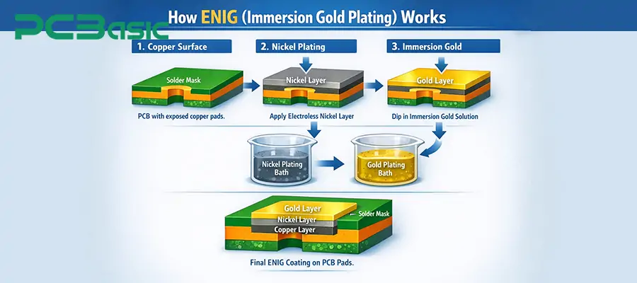
ENIG plating is a chemical surface treatment process used in the manufacturing of gold-plated PCBs. Unlike electroplating, immersion gold plating does not rely on electric current throughout the process. Instead, it forms a nickel-gold structure on the exposed copper surface through a series of controlled chemical reactions.
The ENIG process usually consists of the following three main steps.
Copper Activation
Before conducting metal deposition, the exposed copper pads on the gold-plated PCB need to undergo thorough cleaning and activation treatment to remove the oxide layer, contaminants, and residues from the previous process. This step provides a stable and uniform attachment foundation for the subsequent metal layer. If the activation of the copper surface is not properly controlled, it will directly affect the overall reliability of the PCB's gold plating surface.

Electroless Nickel Deposition
After the copper surface activation is completed, a layer of nickel is deposited on the copper surface through a chemical reaction. This process does not use an electric current, so the nickel layer can be uniformly formed in all exposed areas. In plated gold PCB assemblies, the nickel layer is a key structural layer, and its common thickness is approximately 3–6 µm. Its main functions include:
As a diffusion barrier layer between copper and gold
Providing the necessary mechanical strength
Forming an actual weldable interface during assembly
In a gold-plated circuit board, it is precisely this layer of nickel that actually participates in the formation of the solder joints.
Immersion Gold Plating
After the nickel layer is formed, an extremely thin gold layer is deposited on its surface through a displacement reaction. During the immersion gold plating process, gold ions replace a small portion of the metal on the nickel surface, thereby forming a uniform gold coating. In ENIG plating, the thickness of the gold layer is usually relatively thin, typically ranging from 0.05 to 0.1 µm. Its main function is to prevent the nickel layer from oxidizing before soldering and to provide a stable surface condition for the gold plated PCB assembly.
In the finished gold-plated PCB, the gold layer itself does not form a soldering point structure. During the reflow soldering process, the gold will rapidly dissolve into the solder. The solder then directly reacts with the nickel layer, forming a true metallurgical bond. In the ENIG plating structure, the gold mainly serves as a protective layer, while the nickel layer is the core interface that determines the reliability of the plated gold PCB assembly's soldering points.
|
Item |
ENIG (Immersion Gold Plating) |
Electroplated Gold PCB |
|
Gold deposition method |
Chemical displacement (immersion gold plating) |
Electroplating with electrical current |
|
Uses electrical current |
No |
Yes |
|
Gold thickness |
Thin, typically 0.05–0.1 µm |
Thicker, controllable based on requirements |
|
Surface flatness |
Very flat and uniform |
Relatively less flat |
|
Soldering performance |
Stable, suitable for SMT assembly |
Not typically used as the primary soldering surface |
|
Mechanical wear resistance |
Moderate |
Excellent |
|
Typical applications |
Solder pads, BGA, QFN, SMT areas |
Gold fingers, edge connectors, contact areas |
|
Cost structure |
Relatively cost-effective |
Higher cost |
|
Common positioning |
Solderable surface finish |
Functional/contact gold plating |
Based on the assembly method of the circuit board, the usage environment, and whether there is mechanical wear, we can choose different types of gold-plated circuit boards. Although ENIG and electroplated gold both belong to PCB gold plating, their application focuses are very distinct.
Immersion gold plating is mainly used in scenarios where the soldering quality, surface flatness, and assembly reliability are of high importance. Common applications include:
Consumer electronic products assembled using SMT
Industrial control boards with dense wiring
Medical electronics with high requirements for solder joint consistency
Automotive electronic circuit boards with multi-layer structure
High-density SMT components using BGA, QFN or fine-pitch devices

Among these applications, the core requirement is to obtain a smooth, oxidation-resistant, and suitable for soldering surface. Therefore, ENIG is widely regarded as the conventional choice for gold-plated PCBs that are mainly for mounting.
Electroplated gold PCB is mainly used in scenarios where mechanical durability and contact reliability are of greater importance. Typical applications include:
The gold pins on the expansion card
The back panel connector
Memory module
The interface area that needs frequent insertion and removal or contact
In such applications, the thicker gold layer formed through the gold plated PCB process can maintain stable electrical contact even under repeated mechanical wear. If the ENIG or other PCB gold plating processes are mistakenly selected in high-wear areas, it often leads to premature failure or unnecessary rework costs.
Choosing the appropriate gold-plated PCB surface treatment method hinges on understanding the functional positioning of the circuit board in the actual product, rather than merely considering "whether to use a gold surface". First and foremost, it is necessary to clarify that the primary function of the gold layer is for soldering or for contact.
In the following situations, immersion gold plating is usually a more suitable option:
The circuit board is assembled using SMT technology.
There are specific requirements for the surface flatness.
The gold layer is mainly used to prevent oxidation, rather than to withstand wear.
The surface treatment of the entire board needs to take into account cost control.
In the following scenarios, it is more suitable to choose electroplated gold PCB:
The board is equipped with gold fingers or connector interfaces.
It needs to withstand repeated plugging and unplugging or sliding contacts.
There are clear requirements for mechanical wear resistance.
There is a precise control demand for the thickness of the gold layer.
In actual design, many gold-plated circuit boards will adopt both of these methods simultaneously: the pad areas use ENIG, while gold plating is only applied in specific contact areas. This combined PCB gold plating solution can achieve a more reasonable balance between reliability, performance and cost. In the end, choosing the appropriate gold-plated PCB process should be based on the actual application requirements, rather than the surface color or the name of the process itself.
Gold-plated PCB is a general term for various gold-plating processes. This article mainly introduces two methods: electroless gold plating and electroplating gold. As described in this article, these two methods have essential differences in the formation of the gold layer, thickness control, and their actual functions on the circuit board.
The core purpose of the ENIG process is to provide a flat and oxidation-resistant soldering surface for SMT assembly. Electroplating gold is more commonly used in functional contact areas. In practical applications, many circuit boards will adopt both electroless gold plating and electroplating gold processes. They will use ENIG in the areas requiring soldering and locally adopt electroplating gold in specific contact areas to achieve a reasonable balance between performance and cost.
Time is money in your projects – and PCBasic gets it. PCBasic is a PCB assembly company that delivers fast, flawless results every time. Our comprehensive PCB assembly services include expert engineering support at every step, ensuring top quality in every board. As a leading PCB assembly manufacturer, we provide a one-stop solution that streamlines your supply chain. Partner with our advanced PCB prototype factory for quick turnarounds and superior results you can trust.


Assembly Enquiry
Instant Quote
Phone contact

+86-755-27218592
In addition, we've prepared a Help Center. We recommend checking it before reaching out, as your question and its answer may already be clearly explained there.
Wechat Support

In addition, we've prepared a Help Center. We recommend checking it before reaching out, as your question and its answer may already be clearly explained there.
WhatsApp Support

In addition, we've prepared a Help Center. We recommend checking it before reaching out, as your question and its answer may already be clearly explained there.