Global high-mix volume high-speed PCBA manufacturer
9:00 -18:00, Mon. - Fri. (GMT+8)
9:00 -12:00, Sat. (GMT+8)
(Except Chinese public holidays)
Global high-mix volume high-speed PCBA manufacturer
9:00 -18:00, Mon. - Fri. (GMT+8)
9:00 -12:00, Sat. (GMT+8)
(Except Chinese public holidays)
HomePage > Blog > Knowledge Base > PCB Failure Analysis: Identifying, Analyzing, and Preventing PCB Failures
Printed Circuit Boards (PCBs) are the most fundamental and crucial part of electronic products. On the one hand, it is used to fix and support electronic components; on the other hand, it undertakes the role of transmitting electrical signals. Whether it is consumer electronics, industrial automation equipment, automotive control systems or medical devices, whether the products can operate stably for a long time directly depends on the quality and performance of the circuit boards.
Although there have been significant advances in materials, design software and manufacturing processes in recent years, PCB failure is still a common issue in actual production and application. With the continuous development of electronic products towards miniaturization, high density and high performance, the risk of PCB damage, abnormal PCB operation, and hidden defects that are difficult to detect with the naked eye is also constantly increasing. In many cases, even a seemingly minor PCB fault can lead to system malfunctions, safety risks, and even result in high costs such as rework or recall.
Therefore, PCB failure analysis has become particularly important in electronic manufacturing. Unlike simple repair, printed circuit board failure analysis focuses more on understanding why failures occur by identifying the true root causes and failure mechanisms, and finally, fundamentally avoiding the recurrence of similar problems.
This article will focus on PCB failure analysis, combining failure analysis techniques in actual production, common PCB defects, and mature and effective prevention methods to systematically sort out the PCB failure issues and provide engineers and manufacturing manufacturers with a clear and practical reference framework.
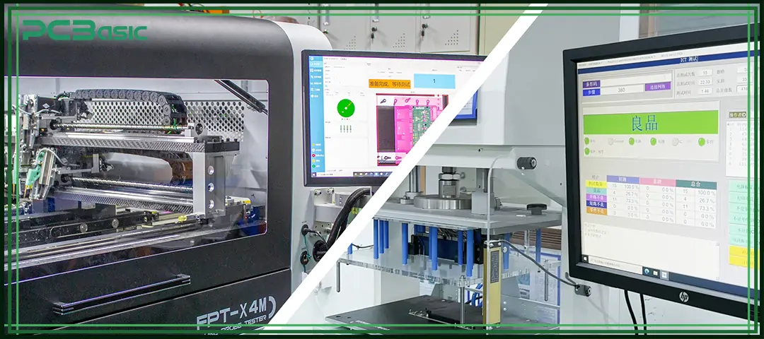
PCB failure analysis is a systematic engineering analysis method, mainly used to identify the true causes of PCB failure. During the analysis process, visual inspection, electrical testing, material analysis, and various microscopy analysis techniques are usually combined to determine why the printed circuit board cannot work properly as originally designed.
Unlike simple troubleshooting, printed circuit board failure analysis pays more attention to the nature of the problem, such as:
• How did the failure occur?
• Which physical, electrical, or chemical mechanisms caused the issue?
• How can effective solutions be implemented to address similar PCB problems in future designs or mass production?
By systematically applying various failure analysis techniques, engineers can turn a single failure into valuable improvement data, thereby continuously enhancing the reliability of the product and the overall manufacturing quality.
Most PCB failures usually result from one or more of the following factors:
|
Failure Source Category |
Specific Causes |
Explanation |
|
Design-related issues |
Insufficient spacing, poor thermal design, impedance mismatch, and incorrect material selection |
Problems introduced during the design phase often escalate later, ultimately leading to PCB failure |
|
Manufacturing defects |
Over-etching, drill misalignment, plating voids, contamination |
Poor process control during fabrication can result in various PCB defects |
|
Assembly problems |
Soldering defects, component misalignment, residual flux |
Common issues during assembly that may lead to a PCB fault |
|
Environmental factors |
Moisture, corrosion, vibration, temperature cycling |
Long-term environmental stress can cause progressive PCB damage |
|
Operational stress |
Overvoltage, overcurrent, mechanical shock |
Operating beyond design limits can accelerate PCB failure |
These factors often interact, turning originally small PCB defects into gradually serious failures over long-term use.
When conducting PCB failure analysis, it is crucial to understand the time points when failures occur:
|
Failure Stage |
Common Issues |
Characteristics |
|
PCB fabrication stage |
Inner-layer defects, plating issues, material flaws |
Root manufacturing-related problems typically identified during PCB failure analysis through cross-sectioning or X-ray inspection |
|
Assembly stage |
Solder joint cracks, pad lifting, component damage |
Often associated with thermal stress or inadequate process control |
|
Testing stage |
Latent electrical faults exposed under stress testing |
Considered “hidden defects” that may not be visible during initial inspection |
|
Field operation stage |
Thermal fatigue, corrosion, electromigration leading to PCB damage |
Typically long-term degradation, where abnormal PCB behavior may appear only after extended use |
Many abnormal PCB behaviors often appear after prolonged use, so accurately identifying the root cause of failure is particularly crucial.
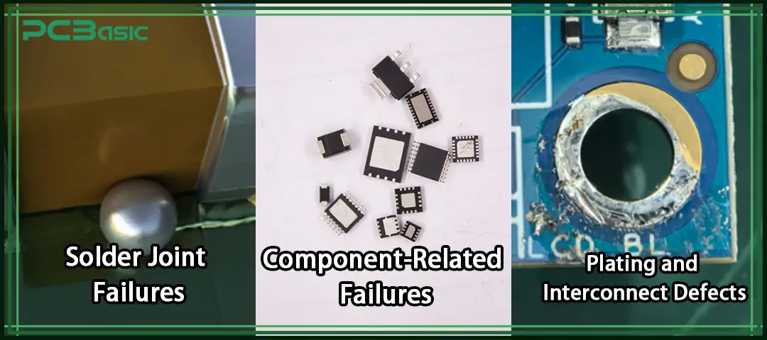
Solder joint issues are one of the most common causes of PCB failure. Cracks, internal voids, cold solder joints, or fatigue caused by long-term thermal cycling and vibration can all lead to poor electrical contact. Sometimes appears as intermittent malfunction, and sometimes it directly leads to a complete PCB fault.
Broken traces, lifted pads, and incomplete through-hole platin can all cause open circuits. Solder bridges, surface contamination or CAF (conductive anodic filament) growth may cause short circuits. These problems are typical printed circuit board defects. Many times, it is difficult to detect with the naked eye and usually requires X-ray or electrical testing for confirmation.
Overvoltage, aging components, counterfeit parts or incorrect component selection can all lead to PCB failure. In actual work, problems are often blamed to the circuit board itself, but the real cause might be the insufficient component reliability or unstable part quality.
Poor thermal design, insufficient thermal relief (starved thermals), or uneven copper distribution will all cause localized temperature to rise. Long-term thermal stress can accelerate PCB damage, such as delamination, racked solder joints, or reduced long-term reliability.
Problems such as plating voids, barrel cracks, and inner-layer separation can affect electrical continuity. Such hidden PCB defects are often not easily detected directly and are the key objects to be investigated in printed circuit board failure analysis, especially more common in multilayer boards.
Moisture, ionic contamination, flux residues and corrosive environments can all cause leakage current, corrosion and even electromigration problems. Such PCB problems and solutions often require a combination of chemical analysis or surface analysis methods to identify the true cause.
Problems such as board warpage, pad lifting, delamination, and measling are mostly related to mechanical stress or mismatched material expansion rates. This type of PCB damage not only increases the difficulty of assembly but may also affect the yield and subsequent reliability.
In high-speed circuit designs, impedance mismatch, crosstalk, electromagnetic interference (EMI), and signal reflection problems are all relatively common. These electrical PCB faults may not immediately shut down the system, but they will gradually affect performance and even leave long-term hidden dangers.
Establishing a clear and standardized workflow is the foundation of conducting an effective PCB failure analysis. This not only enhances the analysis efficiency but also avoids secondary damage to the samples during the detection process, which could otherwise affect the judgment results.
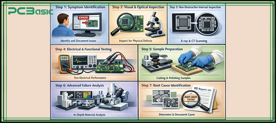
The first step in analysis is to clarify the problem. Common symptoms include functional malfunction, intermittent failure, visible changes, or localized overheating.
Recording the symptoms clearly can help us narrow down the possible causes of PCB failure and avoid blind disassembly or excessive testing.
Next comes basic inspection. Obvious visible problems such as corrosion, contamination, cracked solder joints, and other visible issues can be detected by the naked eye, magnifiers or optical microscope. This step can often directly identify some PCB defects.
If there are no obvious problems with the appearance, further internal inspection is required. Hidden problems such as voids, delamination, or internal cracks can be discovered without damaging the circuit board through X-ray or scanning acoustic microscopy.
Through continuity testing, in-circuit testing (ICT), and full functional testing, it can be confirmed whether there are electrical PCB faults, and it can be determined whether the problem is an open circuit, short circuit, or component failure.
When a deeper analysis is required, sample preparation is extremely crucial. If cutting or polishing is not operated properly, defects may be artificially introduced, which affects the judgment result of printed circuit board failure analysis. Therefore, this step must be carried out carefully.
When it is confirmed that in-depth research is needed, more professional failure analysis techniques can be used, such as:
• Using SEM and SEM-EDS to examine microstructural morphology and elemental composition
• Using XPS to analyze surface chemistry and oxidation conditions
• Using FT-IR to detect organic contamination
• Using DSC and TMA to evaluate thermal properties and material behavior
These means can help us identify the real cause from the microstructural and material levels.
Finally, all the test results need to be summarized, compared and analyzed to confirm the true root cause of the failure. A complete and clear report can ensure that subsequent improvement measures truly address the essential causes of PCB failure, rather than merely dealing with surface phenomena.
Time is money in your projects – and PCBasic gets it. PCBasic is a PCB assembly company that delivers fast, flawless results every time. Our comprehensive PCB assembly services include expert engineering support at every step, ensuring top quality in every board. As a leading PCB assembly manufacturer, we provide a one-stop solution that streamlines your supply chain. Partner with our advanced PCB prototype factory for quick turnarounds and superior results you can trust.
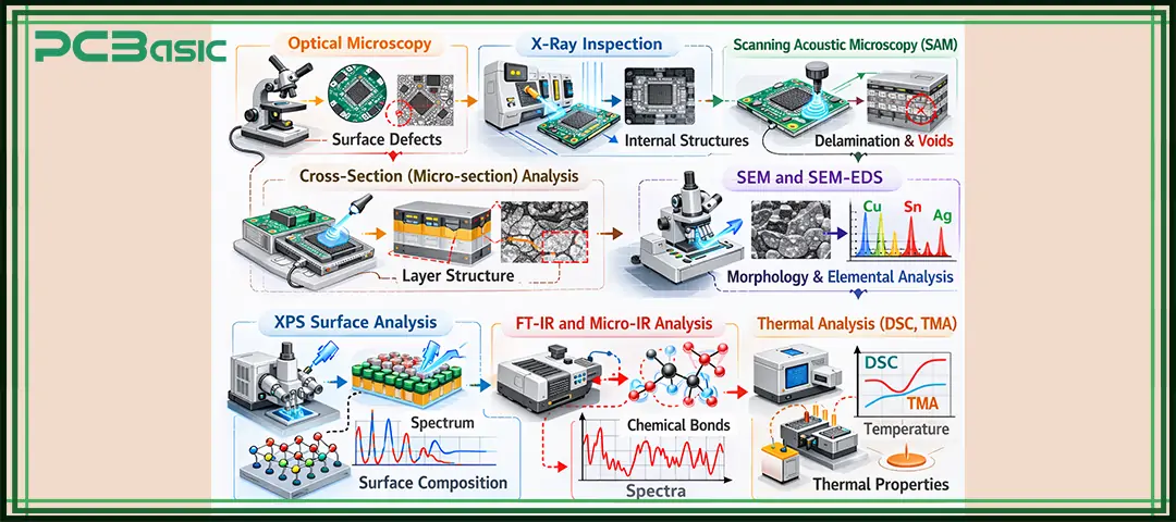
|
Analysis Technique |
Primary Purpose |
Typical Applications |
|
Optical Microscopy |
Detect surface defects and assembly issues |
Used to identify corrosion, cracks, contamination, and visible PCB defects |
|
X-Ray Inspection |
Analyze internal structures and solder joint integrity |
Essential for inspecting BGA solder joints, via defects, and internal interconnect problems |
|
Scanning Acoustic Microscopy (SAM) |
Detect delamination and internal voids |
Used to identify delamination, internal bubbles, and moisture-related PCB damage |
|
Cross-Section (Micro-section) Analysis |
Examine internal microstructures |
A destructive method used to evaluate barrel quality, plating thickness, and internal cracks |
|
SEM and SEM-EDS |
High-resolution imaging and elemental analysis |
Core tools in PCB failure analysis for microstructural observation and material composition analysis |
|
XPS Surface Analysis |
Analyze surface chemical states |
Ideal for investigating oxidation, corrosion, and contamination affecting solderability |
|
FT-IR / Micro-IR Analysis |
Identify organic contamination |
Used to detect flux residues or other organic contaminants causing abnormal PCB behavior |
|
Thermal Analysis (DSC, TMA) |
Evaluate material thermal properties |
Used to measure glass transition temperature (Tg), curing quality, and thermal expansion characteristics for reliability assessment |
Proper layout, controlled impedance, adequate spacing, and solid thermal design can effectively reduce the risk of PCB failure. Thorough consideration during the design stage is the key to avoiding problems later on.
The selection of the right laminate, surface finish, and solder alloy directly affects the long-term reliability of the product. Improper material selection can easily lead to PCB damage or performance degradation in the later stages.
Strict process control, maintaining good cleanliness and adhering to IPC standards can reduce the generation of PCB defects. Many problems often stem from production details.
Through ICT, functional testing, burn-in, and environmental stress testing, PCB faults can be detected in advance to prevent problems from entering the market.
PCB failure analysis is not merely a tool for troubleshooting problems; it is an essential part of quality control in itself. As long as the common causes of PCB failure are clarified, various failure analysis techniques are reasonably used, and combined with the preventive measures in the early stage, PCB damage can be effectively reduced, and the production yield can be improved. It can also make the product more stable.
Conducting a systematic printed circuit board failure analysis is essentially turning each failure into an opportunity for improvement. The more thoroughly a problem is solved, the lower the probability of subsequent problems occurring, and the easier it is for an enterprise to achieve long-term stable development in the field of electronic manufacturing.
Q1: What is the most common cause of PCB failure?
Solder joint defects and thermal stress are among the most common causes of PCB failure.
Q2: Can PCB failure analysis prevent future problems?
Yes. Effective PCB failure analysis identifies root causes and supports design and process improvements.
Q3: Are all PCB defects visible to the naked eye?
No. Many printed circuit board defects require X-ray, SEM, or other advanced failure analysis techniques.
Q4: When should destructive analysis be used?
Destructive methods like cross-sectioning should be used only after non-destructive options are exhausted.

Assembly Enquiry
Instant Quote
Phone contact

+86-755-27218592
In addition, we've prepared a Help Center. We recommend checking it before reaching out, as your question and its answer may already be clearly explained there.
Wechat Support

In addition, we've prepared a Help Center. We recommend checking it before reaching out, as your question and its answer may already be clearly explained there.
WhatsApp Support

In addition, we've prepared a Help Center. We recommend checking it before reaching out, as your question and its answer may already be clearly explained there.