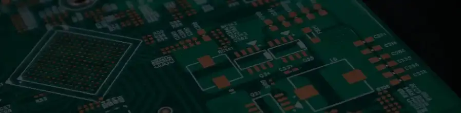
PCBasic PCB Capabilities
PCBasic is located in Shenzhen, China. It is a professional manufacturer specializing in rapid PCB prototyping, assembly (PCBA), and small-batch production.
We have 9 fully automatic SMT assembly lines and are equipped with advanced devices such as AOI, 3D X-ray inspection and flying probe testing to ensure the high quality of each circuit board.
The following is an introduction to the main PCB manufacturing capabilities of PCBasic. Here you can learn about the types of materials we can process, manufacturing processes, product categories, as well as the dimensional accuracy and process tolerances we can achieve.
Our PCB services are divided into two major types:
Quick-Turn PCBs
This includes small-batch, fast-delivery circuit boards, custom specification standard PCBs, and fast-order PCBs (Gerber file viewing supported). These services are highly suitable for the product prototype verification and pilot runs.
Advanced PCBs
This represents the highest level of manufacturing capability for PCBasic, including full-specification PCBs, high-precision complex multi-layer boards, and mass production.
In some cases, certain special materials or laminated structures may be temporarily out of stock.
If your PCB requirements exceed the following capabilities, please contact our sales representative. We will provide you with professional technical support and customized manufacturing solutions.
Note: In PCBasic, "Standard PCB" refers to a comprehensive service of advanced PCB + rapid prototyping PCB, which can not only achieve high-performance manufacturing but also ensure fast delivery.
1. Standard PCB Capabilities
|
Items
|
|
Manufacturing Capabilities
|
Remarks
|
|
Number of Layers
|
-
|
1-14 layers
|
For orders above 14 layers, please view
the below "Advanced PCB" or contact our sales rep.
|
|
Material
|
-
|
FR-4, Aluminum, Copper Base
|
For Flex, Rigid-flex, HDI,
Halogen-free, High Tg, etc., please view the below "Advanced PCB"
or contact sales rep.
|
|
Maximum PCB Size(Dimension)
|
-
|
Single-sided PCB and double-sided PCB:
600*1200mm Multilayer PCB: 560*1150mm
(min 3*3mm)
|
Any sizes beyond this dimension, please
view the below "Advanced PCB" or contact sales rep.
|
|
Board
Size Tolerance(Outline)
|
-
|
±0.2mm/±0.5mm
|
±0.2mm for CNC routing, and ±0.5mm for
V-scoring.
|
|
Board Thickness
|

|
0.2-3.2mm
|
0.2, 0.4, 0.6, 0.8, 1.0, 1.2, 1.6, 2.0,
2.4, 2.6, 2.8, 3.0, 3.2mm. Please view the below "Advanced PCB" or
contact us if your board exceeds these.
|
|
Board
Thickness Tolerance(t≥1.0mm)
|
-
|
±10%
|
Normally "+ Tolerance" will
occur due to PCB processing steps such as electroless copper, solder mask and
other types of finish on the surface.
|
|
Board Thickness Tolerance(t<1.0mm)
|
-
|
±0.1mm
|
|
Min
Trace
|

|
0.1mm/4mil
|
Min manufacturable trace is
4mil(0.1mm), Please view the below "Advanced PCB" or contact us if
your board exceeds these.
|
|
Min Spacing
|
Min manufacturable spacing is
4mil(0.1mm), Please view the below "Advanced PCB" or contact us if
your board exceeds these.
|
|
Outer
Layer Copper Thickness
|

|
1oz/2oz/3oz/4oz/5oz/6oz/7oz/8oz
(35um/70um/105um/140um/175um/210um/245um/280um)
|
Also known as copper weight. 35μm=1oz,
70μm=2oz, 105μm=3oz, 140um=4oz, 175um=5oz, 210um=6oz, 245um=7oz, 280um=8oz,
Please view the below "Advanced PCB" or contact us if you need
copper weight greater than 8oz.
|
|
Inner Layer Copper Thickness
|
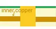
|
1oz/1.5oz/2oz/3oz/4oz
(35μm/50μm/70um/105um/140um)
|
Inner copper weight as per customer's
request for 4 to 10 layers. Please contact us if you need copper weight
greater than 4oz.
|
|
Drill
Sizes (CNC)
|
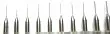
|
0.15-6.0mm
|
Min drill size is 0.15mm, max drill is
6.0mm. Any holes greater than 6mm or smaller than 0.2mm will be subject to
extra charges.
|
|
Min Width of Annular Ring
|

|
0.15mm(6mil)
|
For pads with vias in the middle, Min
width for Annular Ring is 0.15mm(6mil).
|
|
Finished
Hole Diameter (CNC)
|

|
0.15-6.0mm
|
The finished hole diameter will be
smaller than size of drill bits because of copper plating in the hole barrels
|
|
Finished Hole Size Tolerance(CNC)
|
-
|
PTH: +/-0.08mm, NPTH: +/-0.05mm
|
For example, if plated through hole
size is 0.6mm, the finished hole diameter ranges from 0.52mm to 0.68mm will
be considered acceptable.
|
|
Solder
Mask
|

|
LPI
|
Liquid Photo-Imageable is the mostly
adopted. Thermosetting Ink is used in the inexpensive paper-based boards.
|
|
Minimum Character Width(Legend)
|

|
0.15mm
|
Characters of less than 0.15mm wide
will be too narrow to be identifiable.
|
|
Minimum
Character Height (Legend)
|
-
|
0.8mm
|
Characters of less than 0.8mm high will
be too small to be recognizable.
|
|
Character Width to Height Ratio
(Legend)
|
-
|
1:5
|
In PCB silkscreen legends processing,
1:5 is the most suitable ratio
|
|
Minimum
Diameter of Plated Half Holes
|
-
|
0.4mm
|
Design Half-Holes greater than 0.4mm to
ensure better connection between boards.
|
|
Surface Finishing
|

|
HASL with lead, HASL lead free,
Immersion gold, OSP, Hard Gold, Immersion Silver, Immersion Tin, ENEPIG;
|
Please view the below "Advanced
PCB" or contact us for other finishes.
|
|
Solder
Mask
|
|
Green, Red, Yellow, Blue, White, Black,
Matt green, Matte black, Purple, none;
|
No extra charge (Green, Red, Yellow,
Blue)
|
|
Silkscreen
|

|
White, Black, Yellow, None
|
No extra charge (White, Black)
|
|
Panelization
|

|
V-scoring,
Tab-routing,
Tab-routing with Perforation (Stamp
Holes)
|
Leave min clearance of 1.6mm between
boards for break-routing. For V-score panelization, set the space between
boards to be zero.
|
|
Others
|
-
|
Fly Probe Testing (Free) and A.O.I.
testing(free), ISO 9001:2008,UL Certificate
|
No extra charge.
|
2. Advanced PCB Capabilities
|
No.
|
Category
|
PCB
Process Parameters
|
Remarks
|
|
1
|
Multi-layer Boards
|
Standard 3–16 Layers /
Medium 18–24 / High > 24
|
—
|
|
2
|
Blind & Buried Vias (HDI)
|
1 + 1 + N HDI, Any-Layer HDI
|
High-density designs require
thickness-to-diameter review.
|
|
3
|
Surface Finishes
|
HASL, ENIG, OSP, ENEPIG, Hard Gold
Fingers, Partial Gold
|
Partial gold or selective finish
available.
|
|
4
|
Material
|
FR-4, Aluminum, Rogers 4-Series + FR-4
Hybrid, CEM-3
|
Pure PTFE boards require special
lamination process.
|
|
5
|
Drill Diameter Range
|
0.20 – 6.5 mm
|
Below 0.2 mm = HDI via laser process.
|
|
6
|
Aspect Ratio (Thickness : Hole)
|
≤ 8 (Standard), 10 (Medium), 12 (High)
|
> 12 requires special plating
control.
|
|
7
|
Countersink / Counterbore
|
Ø 3.0 – 6.5 mm, Depth Tolerance ± 0.15
mm
|
Non-standard outside range.
|
|
8
|
Hole Position Tolerance
|
± 0.075 mm → ± 0.05 mm
|
< ± 0.05 mm = High Precision.
|
|
9
|
Hole Diameter Tolerance
|
PTH ± 0.075 → ± 0.05 mm / NPTH ± 0.05 →
± 0.025 mm
|
—
|
|
10
|
Hole-to-Hole Spacing
|
Component ≥ 16 mil / Via ≥ 11 mil
|
—
|
|
11
|
Slots & Cut-Outs
|
Plated ≥ 0.5 mm / Non-Plated ≥ 0.8 mm
|
CNC machined.
|
|
12
|
Castellated Holes
|
Diameter ≥ 0.5 mm, Edge ≥ 0.3 mm
|
—
|
|
13
|
Inner Layer Clearance
|
4 L ≥ 7 mil, 6 L ≥ 8 mil, 8 L ≥ 9 mil,
10 L ≥ 10 mil
|
Increase 1 mil for every +2 layers.
|
|
14
|
Inner Layer Min Width/Spacing
|
18 µm Cu → ≥ 4/4 mil
35 µm Cu → ≥ 4/5 mil
|
< 3.5/3 mil = non-standard.
|
|
15
|
Outer Layer Min Width/Spacing
|
18 µm Cu → ≥ 4/5 mil
35 µm Cu → ≥ 5/6 mil
|
< 3.5/3.5 mil requires review.
|
|
16
|
Grid Trace Width/Spacing
|
18 µm Cu → ≥ 7/9 mil
35 µm Cu → ≥ 9/11 mil
|
—
|
|
17
|
Annular Ring (Outer)
|
18 µm Cu → Via ≥ 5 mil, Component ≥ 8
mil
|
Increase with copper thickness.
|
|
18
|
Trace Width Tolerance
|
± 20 % (Standard), ± 10 % (Medium)
|
—
|
|
19
|
Line-to-Edge Distance
|
CNC ≥ 0.25 mm
|
< 0.20 mm needs review.
|
|
20
|
Plating Thickness (ENIG)
|
Ni 100–150 µin / Au 1–8 µin
|
> 8 µin requires quotation review.
|
|
21
|
Hole Copper Thickness
|
Through 18–25 µm / HDI 30–50 µm / High
> 50 µm
|
—
|
|
22
|
Copper Thickness (Layers)
|
0.5 – 4 oz (Standard), 4 – 6 oz
(Medium)
|
> 6 oz = non-standard.
|
|
23
|
Solder Mask Opening & Bridge
|
Opening ≥ 2 mil / Bridge ≥ 4 mil (≥ 4.5
mil for black oil)
|
—
|
|
24
|
Solder Mask Colors
|
Green, Matte Green, Blue, Red, Black,
Matte Black, White, Yellow
|
Special colors available upon request.
|
|
25
|
Etched Copper Legend
|
18 µm Cu → 8 mil width / 40 mil height
|
Adjust by copper thickness.
|
|
26
|
Max Board Thickness
|
Double Side ≤ 4.5 mm / Multilayer ≤ 4.5
mm
|
> 4.5 mm requires review.
|
|
27
|
Min Board Thickness
|
1/2 Layer ≥ 0.3 mm / 4 L ≥ 0.6 mm / 6 L
≥ 0.9 mm / 8 L ≥ 1.2 mm
|
Thinner boards require support panel.
|
|
28
|
Thickness Tolerance (Multi-layer)
|
T≤1.0 ± 0.10 mm / T≥3.2 ± 8 %
|
—
|
|
29
|
Max Board Size
|
508 × 610 mm (Single / Double)
508 × 600 mm (Multi-layer)
|
Larger requires review.
|
|
30
|
Min Board Size
|
≥ 20 mm
|
10–20 mm requires fixture handling.
|
|
31
|
Beveling (Gold Finger)
|
Angle 20° / 30° / 45° / 60°
|
Tolerance ± 5°.
|
|
32
|
Outline Tolerance
|
± 0.10 – 0.15 mm
|
< ± 0.10 mm requires special
control.
|
|
33
|
V-Cut Parameters
|
Angle 30°–45° / Residual Thickness ≥
0.25 mm
|
Below 0.5 mm = single-sided V-cut.
|
|
34
|
Panel Size Range
|
Min 100 × 120 mm / Max 508 × 610 mm
|
< 0.4 mm board ≤ 14 inch panel max.
|
|
35
|
Impedance Control
|
± 10 % (standard), ± 5 Ω for ≤ 50 Ω
lines
|
Controlled per IPC-2141B.
|
|
36
|
Bow & Twist
|
≤ 0.75 % (standard), ≤ 0.5 % (high
precision)
|
IPC Class 2 / 3 compliant.
|
|
37
|
HASL Process Limits
|
Hole > 0.5 mm / Tin Thickness 2–30
µm
|
—
|
|
38
|
Acceptance Standard
|
IPC-A-600 / IPC Class 2 or 3
|
Default Class 2 unless specified.
|
Upload PCB Files (Gerber, .pcb, .PcbDoc, .cam)
Thank you for reviewing the circuit board manufacturing capabilities of PCBasic. When you place an order online, please upload your PCB files in any of the following formats: Gerber, .pcb, .PcbDoc or .cam.
Preferred format: Gerber file (RS-274X/X2 standard).
If you only have the source files of Altium DXP/Altium Designer (.pcb / .PcbDoc), we can also generate Gerber files for you. Our engineering tools support project files of Altium Designer versions 23.x and 10.x. Please try to avoid using versions higher than AD 23.x / 10.x to ensure full compatibility of the files.
You can also send the files directly to your PCBasic sales representative, but we strongly recommend that you place an order and upload the files online through the website. This way, you can enjoy a faster processing speed and complete traceability.
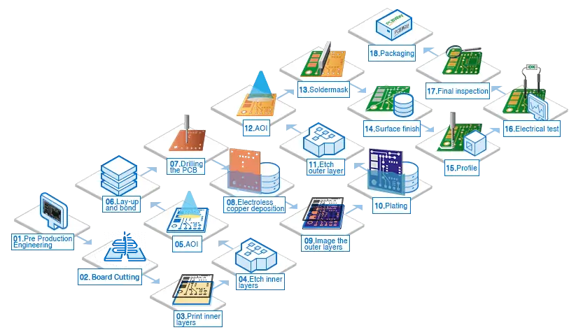
Making a PCB - PCB Manufacture Step by Step
Our Customers
Defense & Smart Devices
We offer circuit board manufacturing services from prototype to mass production for mission-critical electronic products, ensuring high reliability and consistency. Customers choose PCBasic because we have a fast response, strict tolerance control and a stable quality management system.
Medical & Biomedical
Medical customers make up an important part of our customer base. PCBasic strictly adheres to a high-standard quality system, offering short delivery times and competitive prices to meet the manufacturing demands of medical equipment with extremely high repeatability and precision requirements.
Commercial, Industrial & Automotive
Most of our orders come from these industries. PCBasic, with its advantages of rapid quoting, on-time delivery, professional engineering support and high cost-effective manufacturing capabilities, helps customers smoothly expand from small-scale verification to large-scale production.
Universities, Schools & Makers
We support students and electronics enthusiasts - they are the future innovators in technology. PCBasic has become a reliable partner for academic projects, competition projects and maker research and development by offering affordable pricing and stable quality.
If you are engaged in an educational project or team, feel free to send us the project details. We are happy to explore suitable cooperation methods for the educational support program.