Help Center  
Sending a message
Open Hours:9:00-21:00 (GMT+8)
Service hotlines

9:00 -18:00, Mon. - Fri. (GMT+8)

9:00 -12:00, Sat. (GMT+8)

(Except Chinese public holidays)

X

PCB Prototype price calculator | PCB fabrication cost estimator calculator

pcb prototype PCB Specification Selection

Quick order (optional)

* Please upload the Gerber files!

For special requirements not avaliable on this page, please send your requirements and Gerber files to us

and we will come back to you with a price in 2 working days

Material type:

fr4 material FR-4

FR-4

is the most commonly used PCB substrate, composed of woven fiberglass cloth and epoxy resin. It offers excellent electrical insulation, mechanical strength, and heat resistance, making it ideal for the production of double-sided and multilayer PCBs. Its outstanding stability makes it widely used in consumer electronics, industrial control systems, communication equipment, and other electronic applications.
22F 22F

22F

is a paper-based epoxy resin material that combines good processability with low cost, making it suitable for single-sided PCB manufacturing. Its simple drilling and forming characteristics make it a popular choice for budget-sensitive applications with high production volumes, such as low-end consumer electronics, small appliances, and LED lighting.
FR-1 FR-1

FR-1

is the most economical PCB material, made from paper and phenolic resin. It is best suited for simple, low-temperature single-sided PCB designs. Commonly used in low-cost products like electronic toys, chargers, and power adapters, it is not suitable for high-temperature processes such as reflow soldering.
FR-1 Aluminum

Aluminum PCBs

offer excellent thermal conductivity and heat dissipation performance, making them ideal for high-power applications such as LED lighting, power modules, and motor drives. These boards consist of an aluminum base layer, an insulating layer, and a copper foil layer. With their robust structure and high heat resistance, aluminum PCBs help extend the lifespan of electronic components and improve overall system stability, making them the preferred choice for projects with demanding thermal management requirements.

*Material model can be remarked below. HDI is available for 4-layer or more.

Layer count: tip help

Layer count

① The pricing for single-layer and double-layer PCBs is generally similar. However, the cost increases with the number of layers.
② To improve efficiency while ensuring product quality, we use panelized production for both prototypes and mass production.
③ For single-layer boards in mass production, copper will not be retained inside the holes. If copper is required in the holes, please place your order as a double-layer board.
④ When designing single-layer boards, please ensure the engineer pays close attention to avoid reversed traces or silkscreen.

 1   2   4   6   8  10 12 14 16 18 20 22 24 28 30 32

Size (single): tip help
Board size" refers to the length and width dimensions of the delivered PCB.
① For single round boards, the size refers to the diameter of the circle.
② For irregularly shaped boards, the size is calculated based on the maximum width and height.
To reduce costs, we recommend choosing factory panelization for irregular-shaped boards.

X
mm
Please write Length and width!

Quantity: tip help
Board Quantity (pcs): The board quantity refers to the number of boards delivered.
① If delivered as single units, the quantity is based on the number of individual boards. ② If delivered as panelized boards, the quantity is based on the number of panels.
③ The order quantity must be an integer selected from the available options in the ordering system. The actual delivery quantity is subject to the quantity indicated on the factory packaging.

pcs
Please fill in the quantity of panels!

Board type: tip help

Delivery Method

① Single Board Delivery: Refers to cases where the original file is a single board. (Note: If "single board" is selected when placing the order but the file is panelized, we will still process it as a single board by default. The same applies in reverse. Customer complaints will not be accepted in such cases.)
② Customer Panelization: Refers to situations where the customer provides a panelized file or the data is already panelized. 1)For orders without SMT service, if the customer-provided panel does not pose a depaneling risk and has properly designed breakaway tabs and mouse bites, we will follow the provided file directly. 2)For orders requiring SMT assembly, we may adjust the panel by adding tooling edges or modifying fiducial marks to meet our SMT process requirements.
③ Factory Panelization: Refers to cases where the original file is a single board, and the factory is requested to panelize. This option is only suitable for regular-shaped boards or boards requiring SMT with added tooling edges. If you select this option, we will add fiducials and positioning marks by default. The inner connection points will be added based on the board outline. Please specify if you have any special requirements.

Single piece Panel PCB as design Panel by PCBasic

Different designs:

PCB Process Information

>

Thickness: tip help

Board Thickness (mm)

“Finished Board Thickness” refers to the overall thickness of the PCB, and any measurement within the specified tolerance range is considered acceptable.
① Thickness Measurement:For standard PCBs, the thickness is measured at areas where both sides have copper layers covered with solder mask.For boards with gold fingers, the measurement is taken at the area where the gold plating is applied on both sides. (If you have specific requirements regarding board thickness, please indicate them clearly. Otherwise, we will consider it as acceptance of our default specifications.)
② Thickness Tolerance: For finished thickness ≥ 1.0mm: tolerance is ±10%,For finished thickness < 1.0mm: tolerance is ±0.1mm
③ Pricing Notes:The factory considers 0.8–1.6mm as the standard thickness range. Thickness outside this range will incur additional costs, which are subject to the quoted order price. Customers may choose according to their needs.
④ Rogers Material:For pure-pressed double-sided Rogers boards, the base thickness refers to the substrate thickness only. The final finished thickness also includes copper thickness, solder mask, and surface finish layers. The board thickness tolerance is controlled according to IPC standards.

 0.4mm   0.6mm   0.8mm   1.0mm   1.2mm  1.6mm 2.0mm 2.4mm 3.0mm 3.6mm 4.0mm

Outer copper
weight: tip help

Outer Layer Copper Thickness

① For FR-4 double-sided PCBs, outer copper thickness supports 1–15 oz (refer to available options on the official website).
② For FR-4 multilayer PCBs, outer copper thickness supports 1–8 oz (refer to available options on the official website).
③ For aluminum-based, copper-based, and high-frequency PCBs, the default outer copper thickness is 1 oz; other thicknesses depend on the options listed on the official website.
④ For flex PCBs (FPCs), supported outer copper thicknesses are 0.33 / 0.5 / 0.75 / 1 / 2 oz; for other values, please refer to the website's selectable options.

 1oz   1.5oz   2oz   3oz   4oz  5oz 6oz 7oz 8oz 9oz 10oz 11oz 12oz 13oz 14oz 15oz

Solder mask color: tip help

Solder Mask Color

① Green is the default color and does not incur additional charges. Other colors will incur extra fees, typically starting from 50 RMB, depending on the actual cost. If you are ordering expedited boards with non-standard colors, the cost will be higher. Therefore, we recommend choosing green for urgent orders.
② Matte black is considered a special color. It significantly increases the difficulty of troubleshooting circuit or soldering issues and may lead to disputes. We recommend avoiding this option.
③ Since single-sided boards only have circuits on one side, we apply solder mask by default on the circuit side. If solder mask is required on both sides, please contact our customer service.
④ Due to tolerance in each batch of ink mixing, we ensure minimal color variation within the same batch. However, color differences may occur across different batches.

Green White Blue Black Yellow Red Matte Black Matte Green Purple None

Silkscreen: tip help

Silkscreen Color

① Except for PCBs with white solder mask, which use black silkscreen, we only provide white silkscreen by default. For other silkscreen color requests, please contact our sales team for evaluation.
② For single-sided boards with white core material, white silkscreen is not recommended. Using silkscreen as a substitute for solder mask is not accepted.

White Black None

Minimum Trace
Width/Spacing: tip help

Minimum Trace Width/Spacing

Refers to the narrowest width of a single trace and the minimum distance between two adjacent traces in the PCB design.

 3/3mil   3.5/3.5mil   4/4mil   5/5mil   6/6mil ↑  8/8mil ↑ 10/10mil ↑ 20/20mil ↑

Min. drill hole: tip help

Minimum Hole Diameter (mm)

① The smaller the hole diameter, the higher the cost.
② Higher hole density will also increase the cost accordingly:For double-sided PCBs, pricing is based on 80,000 holes per square meter. For 4-layer and above, pricing is based on 100,000 holes per square meter.An additional charge of 4 RMB per 10,000 holes per square meter will apply.

 0.12mm   0.2mm   0.25mm   0.3mm   0.35mm  0.4mm 0.5mm 0.6mm 0.7mm 0.8mm ↑

Test method: tip help

Test method

① 100% Flying Probe Test: Charged per batch. Guaranteed 100% circuit yield.
② Fixture Test (Test Jig): One-time fixture fee; free for repeat orders. Guaranteed 100% circuit yield.
③ 100% AOI (Automated Optical Inspection): Free of charge. Guarantees over 99% circuit yield. For defects within 1%, replacements or refunds will be provided based on the defect ratio. Component, soldering, or other non-PCB-related costs are not covered.
④ Four-Wire Low Resistance Test: Additional charge applies. This test allows micro-ohm level testing of vias, unlike standard fixtures that can only test at ohm levels. It can detect both open vias and potential via issues (commonly referred to as “bad vias”). For surface open/short circuit detection, please also select full circuit testing (100% flying probe or fixture test).
⑤ Fixture Validity Period: Test jigs are stored for up to 12 months. If there is no repeat order within 12 consecutive months, the fixture will be scrapped. Repeat orders after this period will incur a new fixture fee.

 100% flying probe testing   Engineering test frame 

Surface finish: tip help
Pad surface treatment Bare Copper HASL with Lead (Hot Air Solder Leveling with Lead) Lead-Free HASL ENIG OSP Immersion Tin Immersion Silver Electroplated Gold ENEPIG
Effect processing
Process description The copper surface is left untreated with no surface finish applied. Electrical testing is performed directly after the silkscreen process. A process in which molten tin (or tin-lead) solder is coated onto the PCB surface and then leveled using heated compressed air to create a smooth, even finish. A process in which molten tin solder is applied to the PCB surface and leveled using heated compressed air to achieve a smooth and uniform finish. A layer of nickel is first deposited onto the exposed copper surface, followed by a layer of gold with excellent electrical performance. OSP is a process that forms a layer of organic solderability preservative on the clean bare copper surface through a chemical reaction, serving as a protective coating. A copper-tin intermetallic compound formed by depositing a layer of tin (Sn) onto the PCB pad surface through a chemical displacement reaction where tin replaces copper (Cu).4o This process falls between organic coating and electroless nickel/immersion gold, offering a simpler and faster manufacturing method. Metallic nickel and gold are deposited on the pad surface through electrolytic plating to protect the electrical and mechanical properties of the circuit board. Compared with ENIG, ENEPIG adds an additional palladium layer between the nickel and gold layers.
Advantages and disadvantages of the process Advantages: Low cost, smooth surface, and good solderability (when not oxidized).
Disadvantages: Easily affected by acids and humidity; must be used within 2 hours after unsealing, otherwise oxidation may occur.
Advantages: Relatively low cost and good solderability.
Disadvantages: Uneven pad surface, not environmentally friendly (contains lead), and not suitable for fine-pitch pads. If the design includes BGA pads, HASL with lead must not be selected. Any issues such as solder bridging or cold solder joints will not be accepted as complaints.
Advantages: Environmentally friendly to some extent, relatively low cost, and good solderability.
Disadvantages: Less flat compared to ENIG or OSP, not suitable for fine-pitch component soldering, prone to solder ball formation, which may affect soldering quality. If the design includes BGA pads, lead-free HASL must not be selected. Any issues such as solder bridging or cold joints will not be accepted as complaints. 4o
Advantages: Flat surface, suitable for fine-pitch component soldering, supports multiple reflow cycles, and offers good solderability.
Disadvantages: Higher cost, weaker solder joint strength, potential risk of black pad issues, and concerns about long-term reliability.
Advantages: Offers the benefits of bare copper solderability, can be reworked if the surface finish expires (usually no more than twice), low cost, and widely used in BGA and other applications requiring high surface flatness.
Disadvantages: Susceptible to acids and humidity, poor performance during secondary reflow, limited shelf life, and must be used within 24 hours after opening. 4o
Advantages: Provides good solderability similar to HASL and flatness comparable to ENIG, without the intermetallic diffusion issues associated with ENIG.
Disadvantages: Short shelf life; prone to tin whiskers, which may lead to reliability issues due to tin whisker growth and tin migration during soldering.
Advantages: Immersion silver offers excellent electrical performance, superior flatness, and good contact properties unmatched by other surface finishes. It is commonly used in communication, automotive, computer, high-speed, and high-frequency applications.
Disadvantages: Immersion silver is prone to issues such as loss of luster and solder joint voids.
Advantages: Excellent conductivity for stable signal transmission; strong oxidation resistance extends product lifespan; dense and wear-resistant plating is suitable for applications involving frequent plugging and unplugging.
Disadvantages: Higher cost increases overall product expense; relatively weak solder joint strength; when using electroless nickel processes, there is a risk of black pad, which may affect long-term reliability.
Advantages: Widely applicable and effectively prevents black pad issues.
Disadvantages: Palladium is expensive, and the process requires strict control.
Suggested storage conditions ① Vacuum packaging ② Warehouse temperature: 22±4°C ③ Warehouse humidity: 30%RH–60%RH ④ After sealing, cartons must be stored off the ground and away from walls in a dry, well-ventilated area, avoiding direct sunlight.
Vacuum packaging shelf life 3 months 6 months 6 months 6 months 3 months 3 months 3 months 6 months 6 months
Optimal welding conditions ① After vacuum packaging, soldering should be completed within 12 hours. Otherwise, it is recommended to bake the boards before SMT (at 105°C for 2 hours). ② Bare copper boards and OSP-treated boards must not be baked.

 Bare copper   HASL with lead   HASL lead free   ENIG (Immersion Gold)   OSP  Immersion Tin Immersion silver Electroplated gold ENEPIG Immersion gold 2U+OSP Lead-Free HASL + Selective ENIG Lead-Free HASL + Selective Electroplated Gold

Impedance control: tip help

Impedance Control

1. If impedance control is required for the board, please be sure to select “Yes” and choose a stack-up structure that matches the impedance requirements.
2. If there is no impedance requirement, but a specific stack-up is required, you must also select “Yes” and choose the specified stack-up. Default stack-up is free of charge, but custom stack-up will incur additional cost.
3. If there is no impedance requirement and no stack-up requirement, select “No”, and we will use our standard stack-up by default.
4. If you're unsure whether impedance control is required, be sure to consult with your engineer. Selecting the wrong stack-up may result in impedance out of tolerance.
5. Whether impedance control is required or not, the stack-up will not be changed for repeat orders.

 Yes   No 

* Specify impedance trace locations and values in the document, and upload with PCB files.

Profiling Method tip help

Profiling Method

1. Mold Forming: Suitable for high-volume production. The PCB is shaped using stamping molds. Advantages: Low cost and fast processing speed. (Minimum charge: 2000 RMB per design; complex outlines may incur additional costs.)
2. Mechanical Routing: Ideal for small batches or complex board shapes, using CNC machines for precision cutting. Advantages: High accuracy and flexibility. Disadvantages: Lower efficiency and higher cost. (For FR-4 boards: If routing length exceeds 80 meters per square meter, additional charge is 0.4 RMB/m² per meter; For metal-based boards: If routing length exceeds 40 meters per square meter, additional charge is 1 RMB/m² per meter.)
3. V-CUT Scoring: V-grooves are made on the PCB to allow customers to separate the panel into individual pieces after assembly. V-CUT is available in manual and automatic options, with automatic V-CUT offering higher precision.

Mechanic molding

Pre-Plating process:

Electroless copper plating

PCB Shipping Requirements

>

Quality
compensation: tip help

Quality Compensation Service

I. Component Compensation Service

When selecting the component compensation service, a quality assurance service fee will be charged. Service Fee (minimum charge of 20 RMB): Service Fee = PCBA Unit Cost × 0.005 × Order Quantity Example: 100 units, unit cost 100 RMB → Service Fee = 100 × 0.005 × 100 = 50 RMB

II. Compensation Amount

Compensation is based on the actual unit cost of the PCBA, with a maximum of 500 RMB per unit. For a single order, the maximum compensation is 500,000 RMB.

III. Compensation Conditions

Only applies to quality issues caused during production, including: Open circuits, short circuits, intermittent vias (via seems connected but is not), via discontinuity issues caused by other reasons (e.g., incorrect engineering files, design errors leading to open/short circuits, outline, solder mask, silkscreen, tolerances, etc.) are not covered. If a specific quality issue is identified, you must contact us immediately. Do not repair the PCBA on your own, as repairs may prevent issue verification and invalidate compensation eligibility. Only issues occurring under normal environmental conditions are covered. Problems resulting from special environments are excluded from compensation (including but not limited to strong acids, strong alkalis, high temperatures, or extreme cold). If the issue is confirmed to be a quality defect, the PCBA ownership will revert to the factory. Once the faulty PCBA is returned to us, compensation will be processed within one week.

Notes: If you have concerns about PCB quality, please raise them within 6 months from the delivery date. Claims beyond this period will not be accepted.
To ensure full compensation for components under this paid service (specific quality assurance), 4-wire low-resistance testing is required.

According to standard product contract Full component compensation (Exclusive to premium orders)

Four-Wire resistance
test for vias: tip help

4-Wire Low-Resistance Via Testing

1. Military and automotive PCBs must undergo 100% 4-wire low-resistance testing. If your board is a low-cost consumer product, we recommend not selecting this option. However, if it is a high-value product or a military/automotive board where zero PPM risk is required, this test is strongly recommended.
2. 4-wire low-resistance testing can detect micro-ohm-level resistance in vias, while standard fixtures can only perform ohm-level testing. This method not only identifies fully open vias but also detects hidden via defects (commonly known as “bad vias”). For surface open/short circuit testing, please also select full circuit testing.
3. Pricing:Due to slower speed and higher cost, the minimum charge is 100 RMB.
An additional 80 RMB per square meter applies. 4. Intermittent vias or latent via defects cannot be detected by standard testers. For products with high value or reliability requirements, it is recommended to use this test method to eliminate such risks.

None Full Testing

Project file confirm: tip help

Production File Confirmation

Production file confirmation is a service where the factory provides customers with the final manufacturing files for review before PCB production begins. This option can be selected when placing your order.
1. If you choose “Require Production File Confirmation”, the factory will notify you to review the production file after payment confirmation. The lead time will be recalculated starting from the time the production file is confirmed. Confirmation is done via the DFM Order Assistant, which provides realistic simulation images for a clearer view of the final PCB appearance.
2. If you select “Not Required”, the system will generate the production file from your submitted source files and proceed directly to production without confirmation.
3. To prevent misuse of this feature, a symbolic fee of 5 RMB will be charged. Orders over 1㎡ are eligible for free confirmation service.
4. If you do not need the system to confirm the production file, please make sure to select “Not Required” when placing your order.

Yes No

* Production file re-confirmation before order release: ¥5 for orders ≤ 1㎡, free for orders > 1㎡.

Test report: tip help

Test report

Please note that testing reports require processing time and may cause a slight delay in delivery. We appreciate your understanding.

1. Electrical Testing: Primarily checks for open and short circuits in PCB products. Main testing equipment includes flying probe testers and bed-of-nails testers.
2. Final Product Inspection: 
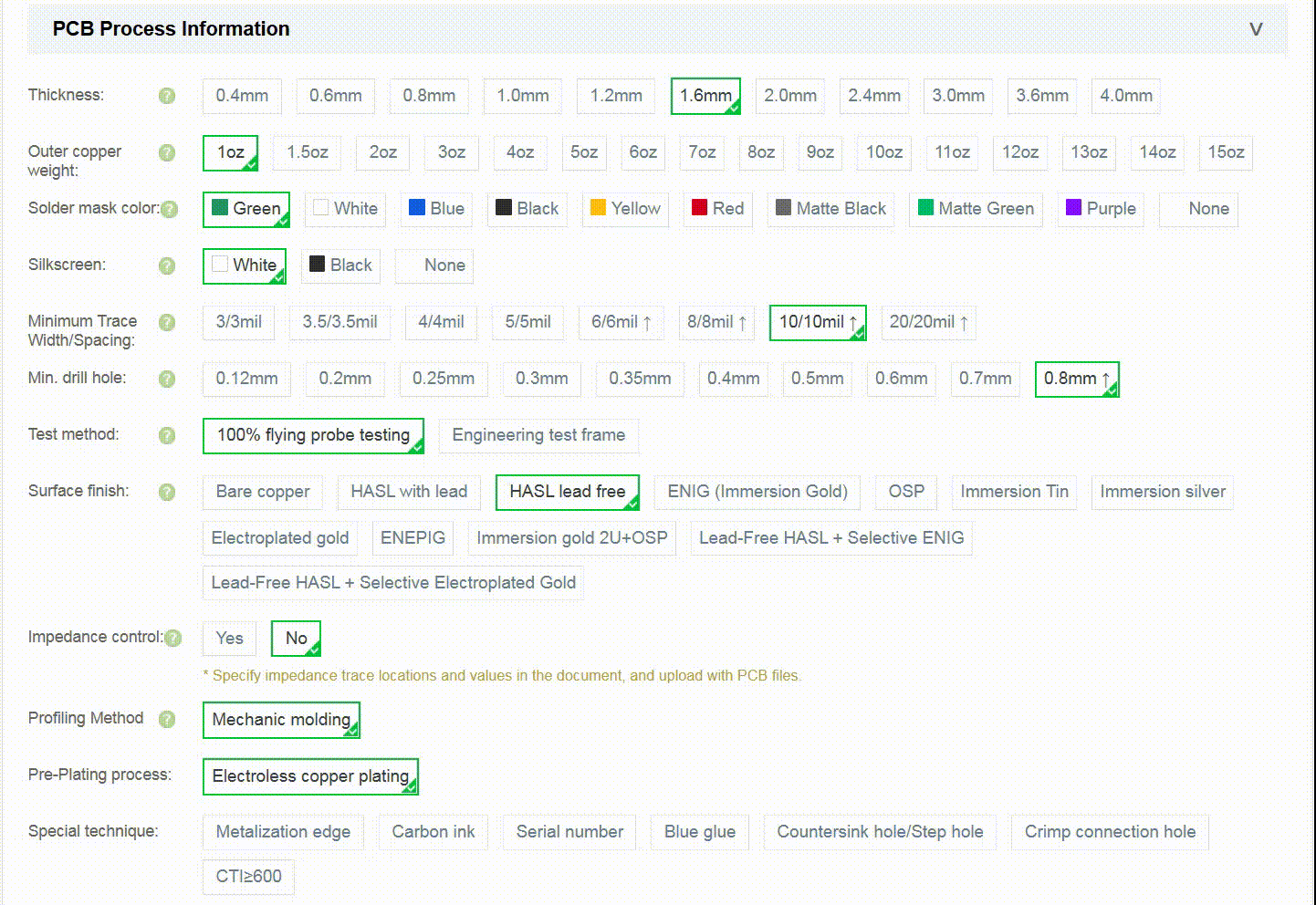
Focuses on visual and dimensional checks, such as appearance, hole size, surface finish compliance, solder mask color, and silkscreen accuracy.
3. Microsection Analysis: Includes inspection of surface copper thickness, plated hole copper thickness, dielectric layer thickness, and internal laminate structure. (Does not include actual potting and slicing of physical samples.)
4. Plating Thickness Test: Measures the thickness of surface finishes, including nickel/gold, tin, tin-lead, and OSP coating thickness.
5. Solderability Test: Preliminary test to assess the solder wetting effect on treated pads and plated through-holes.
6. Ionic Contamination Test: Detects residues from chemical cleaning agents, ambient humidity, fluxes, ionic surfactants, and contaminants such as human sweat that may affect PCB reliability.
7. Thermal Stress Test: Simulates the thermal stress PCBs experience during rapid temperature changes (e.g., from high temperature to room temperature), used to evaluate performance during power on/off cycles and operation.
8. Impedance Report: Includes impedance traces and measured impedance values (does **not include physical impedance coupons). Verifies whether PCB impedance meets customer specifications.

Quality assurance certificate Electric test Final inspection Microsection measurement Surface plating thickness test Solderability test Ionic contamination test Thermal stress test

Test report type:

Electronic Paper

* Please download electronic reports from the “My Orders” page.

Routing outline
tolerance: tip help
Routing Tolerance for Board Outline The main difference between standard routing (standard CNC) and precision routing lies in the positioning method and process flow:
1. Standard routing uses external positioning and performs the routing in a single pass.
2. Precision routing uses internal positioning, involving two routing steps: one rough cut followed by a final precision cut.
Precision Routing Requirements:
1. The design file must include positioning holes, with a minimum diameter of 1.5mm, circular shape (non-plated holes preferred).
2. Use three positioning holes located at different corners for accurate alignment.
3. For single board delivery, the board’s length and width must exceed 5 cm to qualify for precision routing.
4. Off-centered holes cannot be used for positioning; at least two holes must be on opposite sides for proper alignment.
5. For panelized boards, as long as the minimum positioning hole requirements are met, precision routing can be applied.
6. For repeat orders, files will not be re-reviewed. If the original order did not use precision routing, and it is now required, complaints or returns related to this will not be accepted.
Simulation Preview
Note Positioning holes on three sides allow for precision routing. If all positioning holes are located on one side, accurate alignment is not possible and precision routing cannot be performed. It is recommended to use panelization with tooling edges (and add positioning holes on the tooling edges).

Standard routing: ±0.2mm Precision routing: ±0.1mm

IPC level: tip help

IPC level

Surface Appearance Requirements Since IPC Class 2 does not provide explicit specifications for PCB surface appearance, we have established the following simplified standard as an optional personalized service for customers: Scratch Marks – IPC Class 2 Standard:
1. Base material or copper must not be exposed. (According to IPC, repairs are allowed as long as electrical performance is not affected.)
2. Within a 100×150mm area:Only two strip-shaped scratches up to 1×30mm each are allowed.Up to 3 dot-like scratches, each within 1×1mm, are acceptable.
3. Scratched areas must not expose copper, and there should be no obvious whitening under visual inspection. The surface should feel smooth without bumps or dents. Special Reminder: Due to their color characteristics, blue/black or other non-standard solder mask colors make scratches more noticeable. We recommend choosing green solder mask to minimize appearance-related disputes.

IPC-II IPC-III

Interleaving paper: tip help

Interleaving Paper Service

1. What is Interleaving Paper Service? It is a service that places a sheet of white paper between each PCB to prevent surface scratches caused by friction between boards. Target Users: This service is intended for customers who have higher surface appearance requirements. Due to the low processing efficiency, this is offered as a paid, optional service based on customer needs. Pricing:50 RMB engineering fee, Additional 20 RMB/m²
2. Please note:This service cannot be selected if either board dimension is less than 5 cm.

No Yes

Add PO No:

Yes No

Special requirement:

Please fill in the E-mail!
PCB Manufacturing & Pricing
GT Value Build Time Price/Pcs Cost
You can select different parammeters to estimate the cost of the board
 Final price is subject to our review.
Price
$0.00
 Get a discount after submission
$0.00
Excluding Shipping Fees

E-mail

Quote