Heavy Copper PCB Manufacturing-PCBasic
Modern electronics are facing growing power, reliability, and thermal issues; therefore, heavy copper PCBs are emerging as a leading technology solution. Printed circuit boards normally employ copper layers of around 1 oz/ft² in the conventional technology, but heavy copper PCBs employ much heavier copper traces and planes.

Industry professionals characterize a heavy copper PCB as one that consists of 3 oz/ft² (105 μm) or more of copper in its internal or external layers. Some sources add that boards with copper thickness of 2 oz copper (70 μm) can be included as well. These specialized boards usually consist of copper weights of 3 oz to 20 oz/ft², and some extreme versions can reach up to 200 oz/ft².
Heavy copper PCBs obviously have advantages over regular boards. The added weight of copper provides low-resistance pathways to currents in power-thirsty devices that make them more efficient and reduce burnout risk. To take just one example, observe how PCBs of 3 oz copper thickness can handle currents of 10-20 amps reliably for 10 years, while 10 oz types can handle more than 50 amps.
These boards perform exceptionally well in heat management and enable components to run at their best temperatures even in harsh conditions. Their through-hole and connector strength is improved by the robust copper features, thus making them have increased resistance to thermal cycling, vibration, and mechanical stress.
Heavy copper printed circuit board production entails special etching and plating processes. Modern fabrication processes combine plating and etching processes, thus resulting in straight sidewalls with minimal undercut as opposed to previous processes that resulted in rough trace sidewalls. High-current circuits and standard control circuits can now be supported on the same board by manufacturers since they can deposit different weights of copper in the same layer.
This technology addresses increasing consumer demands for electronic products with enhanced heat conductivity, high voltage tolerance, and improved performance in harsh environments.
What is a Heavy Copper PCB (or Thick Copper PCB)?

Standard PCBs contain copper layers of 1oz to 3oz thickness, which is suitable for normal electronics. Heavy copper PCBs (or thick copper PCBs) include copper thickness of 3oz or greater on any or all layers. Some industry experts call boards with copper that exceeds 2oz (70 μm) heavy copper PCBs.
These application-specific PCBs usually have copper from 4oz to 10oz. Super-thick versions are capable of handling extraordinary current loads and go up to 20oz to 200oz per square foot. The increased copper thickness changes the electrical and thermal characteristics of the board.
Heavy copper PCBs are best suited for high-power applications where ultra-high thermal management goes hand in hand with high-power currents. Normal PCBs would not last in such extreme conditions, but heavy copper boards are perfect for managing current flow.
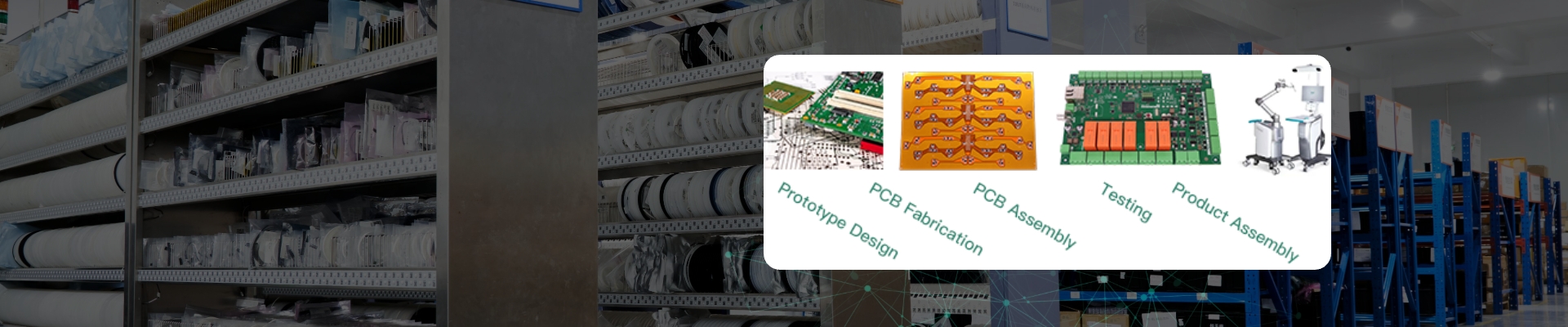
About PCBasic
Time is money in your projects – and PCBasic gets it. PCBasic is the pcb assembly company that delivers fast, flawless results every time. Our comprehensive PCB Assembly Services include expert engineering support at every step, ensuring top quality in every board. As a leading PCB Assembly Manufacturer, we provide a one-stop solution that streamlines your supply chain. Partner with our advanced PCB Prototype Factory for quick turnarounds and superior results you can trust.
Internal Structure of Heavy Copper Boards
Heavy copper PCBs are made with specialized processes above and beyond normal board manufacture. The straightforward process is nevertheless the same - etching and electroplating - but these boards require only special etching and plating techniques. This provides trace sidewalls and undercuts to precise specifications.

Manufacturers use several techniques to build these specialized boards:
● Blue Bar Process
Thick copper bars directly enter the circuit board. This minimizes total weight and enhances plane flatness as resin seeps into copper circuit areas.
● Laminate Deposition
This technique uses a thick copper base for reliability and consistency. It also offers easy edge control for fine traces.
● Buried Copper
Thick copper is pre-installed in the prepreg. Resin thickness and laser cutting are determinants of copper thickness.
Uneven thickness continues to be the biggest technical hurdle in production. Pad positions and layer alignments have to be properly established by fabricators to achieve balanced copper distribution in the board.

Why Heavy Copper PCBs Are Used?
Automotive, power electronics, and industrial equipment require boards that can support rigorous conditions. Heavy copper printed circuit boards were designed to bear such heavy requirements and provide a solution where normal boards will only quickly fail.
Ordinary PCB VS. Heavy Copper PCB

Standard and heavy copper printed circuit boards (PCBs) are mainly different in the copper weight. Normal commercial PCBs use copper weight ranging between 0.5 and 3 oz/ft², which is sufficient for signal transmission but not sufficient for power-hungry designs. Heavy copper PCBs use copper weight ranging between 4 and 60 oz/ft² and thus offer a much stronger platform for power-hungry designs.
|
Feature
|
Ordinary PCB
|
Heavy Copper PCB
|
|
Copper Thickness
|
0.5 oz/ft² to 2 oz/ft²
|
3 oz/ft² to 20+ oz/ft²
|
|
Current Capacity
|
Normal (limited amps)
|
Much higher (ideal for high current)
|
|
Mechanical Strength
|
Standard
|
Very strong and rugged
|
|
Heat Dissipation
|
Moderate
|
Excellent (handles more heat)
|
|
Manufacturing Difficulty
|
Easier, cheaper
|
Harder, more expensive
|
|
Common Applications
|
Consumer electronics, computers
|
Power supplies, automotive, military, industrial systems
|
|
Cost
|
Lower
|
Higher
|
Benefits of Heavy Copper PCBs
The additional copper weight turns an unstable circuit board into a strong and stable wiring platform. Heavy copper printed circuit boards offer low-resistance paths for currents in power-hungry devices and thus enhance efficiency and reduce the risk of burnout.
● High current carrying capacity
Prototyping PCBs of 3oz copper thickness can handle the current of 10-20 amps consistently for more than a decade. 10oz thickness boards can handle more than 50 amps easily. This huge jump in current-carrying ability makes these prototyping PCBs ideal for high-power-density applications.
● Excellent heat dissipation
The additional copper weight serves as a heat sink and dissipates heat from power-intensive components efficiently. This improved thermal management prevents hotspots and enhances system reliability.
● Enhanced mechanical strength at connector sites
TCT (thermal cycle test) shows a tiny 0.57% failure rate after eight cycles for boards with at least 2.5-mil copper plating. This increased mechanical strength makes those PCBs ideal for connector sites and plated through-holes where regular boards fail.
● High reliability in harsh environments
These PCBs are highly resistant to mechanical stresses due to thermal cycling. This excellent durability is the reason for their extensive usage by aerospace, defense, and industrial control applications, particularly when failure is not acceptable.

Design Considerations for Heavy Copper PCBs
Heavy copper PCB design has to be performed with extra care since technical parameters are significantly different from standard PCB design procedures. Numerous important factors have to be taken into account in manufacturing performance, reliability, and manufacturability, particularly when dealing with copper weights over 3 oz/ft².
Copper Thickness and Trace Width

Copper PCB thickness and trace width have a critical relationship in heavy copper PCB design. Minimum trace width must increase as copper thickness does. Standard design rules do not hold anymore—a 3 mil line width adequate for thickness of 0.5 oz copper or 1 oz copper will not suffice for heavier weights. 3-20 oz copper layer boards need traces much wider to be adequately manufactured. More aggressive chemical exposure must be required during etching in thicker copper, so designers need to provide for potential undercut.
How to Choose the Right Copper Thickness
The optimal way of choosing the right copper PCB thickness starts with finding out the current requirements of your application. Trace width calculators are great tools to use in obtaining three such parameters: trace width, current carrying capacity, and temperature rise. The tools can compute the third parameter wherever two parameters are given as inputs, thereby enabling you to select the best copper PCB thickness. Where applications demand current greater than 100A, standard traces are unsuitable and copper bus bars have to be used.

Current-Carrying Capacity
Current capacity has a mathematical correlation with PCB copper weight and trace size. IPC-2221 provides us with the formula I = KΔT^0.44 × A^0.75, where K is 0.024 for internal conductors and 0.048 for external conductors. Internal layers can support only half the current-carrying capacity of exposed traces. Temperature rise should be between 10-20°C in most applications. Heat due to I²R losses should be dissipated sufficiently to prevent component failure.
Substrate and Insulation Material Selection
PCB Copper weight makes substrate selection more important. Board thickness will need to be more than 1.6mm for 20 oz copper. High copper core PCB use calls for High-Tg materials with comparable CTE. FR-4 works, but metal core PCBs (MCPCB) offer better thermal benefits. Some extreme applications will necessitate special laminates with better thermal conductivity.
Thermal Management & Coefficient of Thermal Expansion (CTE)

CTE (Coefficient of Thermal Expansion) measures how much a PCB expands with temperature, in ppm/°C.
Standard FR-4 laminates have a CTE of 14–17 ppm/°C.
Silicon chip packages have a lower CTE of about 6 ppm/°C.
CTE mismatch between PCB and chips causes stress concentration during temperature changes.
Heavy copper PCBs need minimal CTE mismatch because thick copper generates large thermal forces.
Heavy Copper PCBs Manufacturing Process
Heavy copper PCB manufacturing requires specialized processes that differ significantly from standard PCB production. Regular PCBs use simple etching and plating procedures. Heavy copper boards need advanced techniques to handle extreme copper thickness requirements.
1. Traditional Manufacturing Methods
Traditional methods formed heavy copper features by etching thick copper-clad laminated board material. This resulted in uneven trace sidewalls and excessive undercutting. Modern plating technology now combines plating and etching to create straight sidewalls with minimal undercut.
2. Copper Thickness and Layer Processing
Manufacturers typically etch copper-clad laminates for PCBs with copper thickness under 10oz. They directly etch internal layers on copper-clad laminates. External layers go through additional electroplating to achieve the desired thickness. A 3-oz heavy copper PCB uses 3oz copper clad laminates for internal layers and 2-oz material for external layers. Electroplating adds the remaining copper.

3. Manufacturing for Ultra-Thick Copper PCBs
PCBs with 10oz or greater copper thickness start with red copper foil instead of copper-clad laminates. This foil combines with prepreg to create ultra-thick copper PCBs.
4. Solder Mask Challenges
Solder mask application creates unique challenges in heavy copper manufacturing. Traditional silkscreen printing often leads to uneven solder mask thickness. Ink builds up in circuit corners and around vias. Some manufacturers use electrostatic spraying technology that applies solder mask evenly across the board's surface.
The ability to mix heavy copper with standard features on a single board offers significant manufacturing advantages. This combination reduces layer count, provides low impedance power distribution, and creates smaller footprints with potential cost savings. High-current circuits and their control circuits once needed separate boards. Now they combine smoothly to create highly dense yet simple board structures.
Strict process controls and complete testing ensure these specialized boards meet high-power applications' requirements.
Applications of Heavy Copper PCBs
Heavy copper PCBs are essential in industries where regular circuit boards can't handle the electrical, thermal, or mechanical requirements. These specialized boards are the foundations of many mission-critical systems.
1. Automotive Industry

The automotive industry sees thick copper PCBs excel in electric vehicle charging systems and motor controllers. These boards give battery management systems the power to handle currents up to 100 amps during charging and discharging cycles. Their capacity to handle temperatures above 150°C makes them perfect for automotive environments.
2. Power Distribution Systems
Power distribution systems now rely heavily on these PCBs. Companies use them in excitation systems for power regulators, grid switching systems, high power rectifiers, and overload relays. Modern PCB heavy copper boards have replaced older cable distribution and sheet metal methods to streamline processes and boost product reliability.
3. Military and Aerospace Applications
The military and aerospace sectors depend on these specialized PCBs for weapons control systems, radar equipment, and monitoring systems. Electronics in avionics and communication systems last longer thanks to their exceptional mechanical performance in harsh conditions.
4. Renewable Energy Systems
Renewable energy systems need heavy copper PCBs more than ever. Solar inverters, wind turbine controllers, and hydroelectric power plant control panels use these boards to manage heavy power loads. To name just one example, a solar inverter handling 5 kW might use traces designed for 30 amps.
5. Medical Equipment

Medical equipment like imaging devices and patient monitoring systems work better with heavy copper flex PCBs' reliability. Industrial automation systems use them in safety systems, welding equipment, and surge protectors where high current and voltage are common.
6. Advances in Manufacturing Technology
Manufacturing technology advances have helped these specialized boards replace traditional transmission methods. This change has made products smaller while making them more reliable.
PCBasic's Heavy Copper PCB Manufacturing Capabilities

PCBasic leads heavy copper PCB manufacturers. Also, PCBasic is the one of the top China heavy copper PCB suppliers. They define their thick copper products as boards with inner or outer PCB copper thickness greater than or equal to 3OZ (105um). Their ultra-thick copper PCBs handle exceptional power needs with boards that exceed 300μm.
The company's advanced manufacturing techniques go way beyond standard circuit board production. The biggest problem in thick copper fabrication comes from substantial drill bit loss due to increased copper thickness. PCBasic uses specialized UC thick copper drill bits to tackle this challenge. Their equipment and optimized drilling parameters create hole walls that stay flat and smooth, even through exceptionally thick copper.
The etching phase plays a vital role in heavy copper PCB production. PCBasic calls it their core technology in circuit manufacturing. The circuit quality becomes harder to maintain as copper thickness increases.
PCBasic has become skilled at screen printing techniques for heavy copper applications. They focus on strong binding forces between solder mask and base material. A solder mask vacuum pump eliminates quality issues from solder mask bubbles, which become more common with thicker copper.
All PCBasic's thick copper PCBs use high TG materials, so they've invested in specialized titanium-plated gong knives. This investment will give a smooth finish to board edges throughout manufacturing.
The R&D department has created complete documentation including "Design and Operation Guidelines for Thick Copper PCB" and "Process Failure Mode Control for Thick Copper PCB". These systems control product design, process parameters, and finished product testing to meet customer requirements.
This comprehensive system makes PCBasic one of the best heavy copper PCB manufacturers that serve reliably in demanding applications. Their products work well in medical devices, industrial automation equipment, automotive systems, high-speed rail, ships, military products, and LED lighting systems.

Conclusion
High copper PCBs are crucial for modern high-power electronics with copper thicknesses of 3oz/ft² or greater. Such boards can manage currents of over 50 amps without sacrificing thermal stability, making them crucial for power-intensive applications.
Heavy PCB copper stands out in heat resolution, increase credibility, and prevent component failure under extreme conditions. This technique replaces old power transmission methods, resulting in small, more efficient products.
Careful current calculations, substrate choices and thermal expansion are required to design heavy copper-PCBs. Specific production procedures, such as etching and plating, are important for their production.
Heavy copper PCB market increasing in sectors like automotive, military, renewable energy, and medical. As electronic systems evolve, advancements in this technology will enhance power density and reliability for future applications.