Global high-mix volume high-speed PCBA manufacturer
9:00 -18:00, Mon. - Fri. (GMT+8)
9:00 -12:00, Sat. (GMT+8)
(Except Chinese public holidays)
Global high-mix volume high-speed PCBA manufacturer
9:00 -18:00, Mon. - Fri. (GMT+8)
9:00 -12:00, Sat. (GMT+8)
(Except Chinese public holidays)
HomePage > Blog > Knowledge Base > A Comprehensive Guide to PCB Testing
electronic product designers or manufacturers, the worst-case scenario is to discover serious malfunctions only after the product has been launched on the market. Even if the product design is reasonable and the assembly is standardized, there may still be problems, especially in the core part of the printed circuit board (PCB). Many electronic products may have hidden defects during the prototype stage. If they are not detected in time through PCB testing, it may lead to rework, recalls, and even economic losses.
To avoid these problems, effective PCB testing methods must be incorporated into the manufacturing process. Through PCB testing, electrical connection problems, poor soldering, or component failures can be detected in advance, thereby ensuring product quality, reducing the risks brought by on-site failures and protecting brand reputation.
This guide will help you understand what PCB testing is and how to test a PCB board, as well as which PCB testing methods are suitable for different stages. Meanwhile, this article will also introduce the commonly used tools for PCB testing and several typical testing methods, including functional circuit testing (FCT Testing), in-circuit testing (ICT), and automated PCB testing. These PCB testing methods can help ensure the reliable performance and safe use of circuit boards, and meet the application requirements of the final product.

PCB testing refers to a comprehensive inspection of the functionality, reliability and structural integrity of Printed Circuit boards (PCBs) before they are officially mass-produced or put into use. This work runs through the entire production process, mainly to detect potential problems as early as possible, such as short circuits, open circuits, missing components, cold solder joints or thermal failure, etc., to prevent faulty circuit boards from entering the market.
Without a systematic PCB testing process, even a minor defect may cause serious problems after the product is put into use. This not only affects the actual performance of the product but may also lead to customer complaints, increase maintenance or rework costs, and even cause damage to the company's brand reputation. As electronic products become increasingly complex and have more functions, the importance of PCB testing in the entire product development process is also growing.
For different types of products, the required PCB testing intensity and testing methods will also vary. For example, industrial control equipment and automotive electronic systems applied in harsh environments such as high temperature, high humidity, and strong vibration often require more comprehensive and stricter PCB reliability testing; while PCBs used in ordinary consumer electronics, only basic functional tests and connectivity checks are required.
All in all, PCB testing plays a very crucial role in ensuring the stable and reliable operation of electronic products, promoting the development of electronic technology, and meeting market quality requirements. Only through high-quality circuit board testing and validation can it be ensured that each PCB meets the design standards, truly achieving high performance, high reliability and high-quality delivery of the product.
The selection of an appropriate PCB testing method depends on multiple factors, including product complexity, production batch size, testing objectives and budget. The following are the most commonly used PCB testing methods for evaluating the performance, functionality and reliability of PCBs at different manufacturing stages.

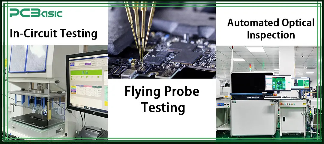
In-circuit Testing (ICT) is currently the most widely used and reliable PCB testing method in electronic manufacturing, especially suitable for high-volume circuit board products with mature designs. It is also known as the Bed-of-Nails Test. Through a test fixture equipped with a large number of spring-loaded probes, it makes individual contact with the fixed test points on the PCB.
In the actual test, these probes will contact the circuit board point-by-point to perform a comprehensive electrical performance test (PCB Electrical Testing). The main inspection contents include:
• Measure basic parameters such as resistance and capacitance;
• Check the polarity and direction of the diode;
• Confirm whether all components have been correctly soldered and meet the requirements of the circuit design;
• Common problems such as short circuits, open circuits, false soldering, poor pads or incorrect installation of components are found.
Typically, ICT testing can cover approximately 85% to 90% of the electrical detection points on a circuit board. The testing process is almost fully automated and does not require manual judgment; thus, the probability of misjudgment and missed detection is extremely low, and the efficiency is also very high.
However, ICT also has its limitations. It has to customize special Test Fixtures for each type of PCB. The development and manufacturing cycle of the fixtures is long, and the cost is high. Therefore, for PCB projects that are in the R&D stage, in small-batch production, or frequently require revisions, ICT testing is not cost-effective in terms of cost and efficiency.
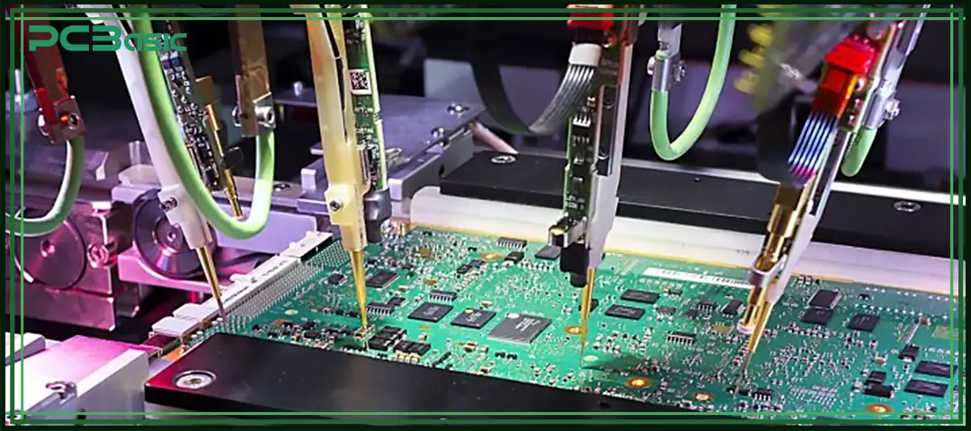
Flying Probe Testing, also known as Fixtureless In-Circuit Testing (FICT), is a highly flexible and low-cost PCB testing method and is often used as an alternative to ICT (In-circuit Testing). It is particularly suitable for the early stage of product development, prototype verification, and small-batch PCB testing.
Unlike traditional ICT, flying probe testing does not use a fixed " bed-of-nails" test fixture. On the contrary, it uses multiple movable probes, which are controlled by software programs and move precisely in the X-Y coordinate system, touching the preset test points on the PCB point-by-point to perform electrical parameter testing (PCB Electrical Testing).
The flying probe testing can detect the following:
• Open circuit and short circuit
• Parameters of devices such as resistors, capacitors and inductors
• Polarity and functional integrity of diodes
Since the PCB is not powered on during the testing process, it is particularly suitable for products that do not meet the power-on conditions or have not yet entered the functional testing stage.
The significant advantage of this method lies in the fact that there is no need to customize test fixtures, which greatly reduces the cost and time of test preparation. It can be adapted to different types of circuit boards simply through software programming, offering extremely high flexibility.
Automated Optical Inspection (AOI) is a commonly used non-contact PCB testing method for appearance inspection, mainly used to check the soldering quality and component placement on the surface of printed circuit boards (PCBs). AOI equipment is equipped with high-resolution 2D or 3D industrial cameras. By capturing PCB images and comparing them with standard templates or design drawings, it can automatically identify various appearance defects generated during the production process.
During the actual testing process, the AOI system will judge and identify the following issues based on the image recognition algorithm:
• Soldering defects, such as excessive solder, insufficient solder, cold soldering, and dry joints;
• Installation errors, such as missing components, misalignment, incorrect orientation, and skewed placement;
• Abnormal connections, such as lifted leads and solder bridges;
• Incorrect parameters, such as component model, polarity direction, and package type mismatch.
AOI detection features fast speed and good repeatability, making it suitable for standard SMT automated production lines. Manufacturers usually place AOI equipment at the workstation after the surface mount technology (SMT) is completed, or before and after reflow soldering, serving as a quality control measure for key stages.
It should be noted that AOI only detects appearance issues while cannot perform power-on operations on the PCB, nor can it determine whether the circuit function is normal. Therefore, AOI itself cannot replace electrical or functional testing methods.

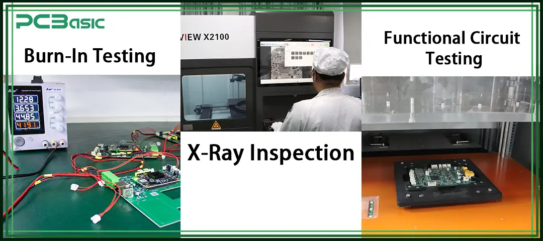
Burn-in testing is a typical method of PCB reliability testing. It mainly simulates the harsh environment that the circuit board may encounter in actual use by applying high temperature, high voltage and high current for a long time. The test duration is usually 48 to 168 hours, with the aim of exposing in advance those faults that are prone to occur in the early stage.
During the testing process, the PCB will be installed on dedicated equipment to run high-load tasks and remain in a full-load state for a long time. The load conditions may even exceed the normal operating range of the product to induce potential problems as soon as possible. This testing method is often used in application scenarios that require high stability, such as aerospace, medical electronics and military systems.
The core functions of the burning testing include:
• Identify infant mortality failures that occur when the product is just put into use;
• Eliminate weak or defective boards PCBs in advance, enhancing the overall quality of shipments and product stability.
In the production of many high-end electronic products, burning testing is an important step before leaving the factory, used to verify whether the PCB can maintain stable operation under extreme working conditions. As one of the commonly used PCB testing methods, it is of great value for ensuring the long-term reliability of products.
Automated X-Ray Inspection (AXI) is a high-precision PCB testing method, mainly used to discover hidden soldering defects inside printed circuit boards (PCBs) and at the bottom of device packages. This method is particularly suitable for complex structures that are difficult to cover by traditional detection methods, such as Ball Grid Array (BGA) packages, flip-chip, and multilayer PCBs.
During the AXI testing process, X-rays can penetrate the PCB and its solder joints to generate images, thereby allowing for the observation of the connection conditions beneath or inside the components. AXI can mainly detect the following problems:
• Cold Solder Joint: the solder is not firmly soldered or the not fully melted.
• Solder Voids: Bubbles or voids inside solder joints that may affect conduction;
• Misalignment under chip packages: Deviation of the solder balls at the bottom of the device or surface mount deviation;
• Barrel defects and broken internal traces: Typical structural defects in multilayer boards.
Unlike AOI, X-ray testing is a non-visual electrical inspection method that can penetrate to positions that are not visible to optical cameras, providing crucial internal structure information. Especially in high-density and high-reliability products, AXI is almost an indispensable testing method.
However, AXI devices are relatively expensive, the testing process is slow, and professional operators are required to analyze images and judge results. Therefore, this method is widely used in industries with extremely high reliability requirements, such as aerospace, automotive electronics, and medical equipment, to ensure the quality of PCB soldering and the stability of the internal structure.
Functional Circuit Testing (FCT), also known as PCB Functional Testing, is a key PCB testing method for evaluating whether the finished circuit board can operate normally under actual application conditions. This test will directly power on the circuit board and simulate the working environment of the final product through external devices, test fixtures and software to conduct a comprehensive functional verification of the entire board.
During the FCT testing process, the testing system will conduct the following checks on the PCB according to the actual application requirements of the product:
• Input/output function test: Confirm whether all interfaces respond normally and communicate stably;
• Power consumption test: Measure the current, voltage and power consumption of the system during operation to see if they are within the design range.
• Analog/digital signal detection: Ensure the accuracy of signal transmission logic and the normal functions of amplification, conversion, filtering and other circuits;
• Operation timing test: Check whether the workflow, delay control, and synchronization logic of the circuit meet the design expectations.
Notice in the early stage is an important link in ensuring product stability and user experience.
However, the preparation work for FCT is relatively complex. Each product usually requires a custom-made dedicated test setup, such as fixtures, programs, and signal simulation modules. The test time is relatively long. Therefore, it is more suitable for complex functions or applications with high-reliability requirements, such as industrial control equipment, communication terminals and automotive electronics.

Time is money in your projects – and PCBasic gets it. PCBasic is a PCB assembly company that delivers fast, flawless results every time. Our comprehensive PCB assembly services include expert engineering support at every step, ensuring top quality in every board. As a leading PCB assembly manufacturer, we provide a one-stop solution that streamlines your supply chain. Partner with our advanced PCB prototype factory for quick turnarounds and superior results you can trust.
In addition to the common functional tests and electrical tests, PCBs in some high-demand applications also need to undergo a series of more rigorous environmental simulation tests and functional tests to further evaluate their performance and reliability under extreme conditions.
Other common test items include:
• Solderability Testing: It is used to verify the wettability of PCB pads and the integrity of solder joints, ensuring the adhesion quality of components during the soldering process and avoiding cold solder or soldering failure.
• Contamination Testing: Check if there are any residual ions on the surface of the circuit board. These contaminants may cause corrosion, leakage or short circuits under humid or high-voltage conditions.
• Micro-Sectioning Analysis: By cross-cutting and microscopic observation of the PCB, it analyzes whether there are internal defects such as delamination, bubbles, cracks, and pad separation in the inner layer structure.
• Time-Domain Reflectometry (TDR): Applicable to high-speed signal PCBs, it can accurately identify signal integrity issues such as impedance discontinuity and reflection interference.
• Peel Test and Solder Float Tests: Evaluate the structural stability and mechanical strength of the PCB under thermal expansion and contraction and high-temperature shock during soldering, and determine whether its heat resistance meets the standards.
These testing methods together constitute an important part of the PCB reliability testing system, which is used to help the engineering team eliminate potential risks in the early stages of product design, verification and mass production.
By rationally combining various PCB testing methods - such as In-Circuit testing, flying probe testing, and functional circuit testing through testing and the various environmental and stress tests mentioned above, manufacturers can comprehensively enhance the quality of PCBS, reduce potential defects, and ensure that each circuit board operates stably and reliably in practical applications.
|
Testing Method |
Function |
Application Stage/Scenario |
Advantages |
Disadvantages |
|
In-Circuit Testing (ICT) |
Checks shorts, opens, resistance, capacitance, and component values |
High-volume production; mature designs |
High coverage (85–90%); fast; low error rate |
High cost; requires custom fixtures; not suitable for frequent design changes |
|
Flying Probe Testing |
Verifies opens, shorts, resistance, capacitance, inductance, diodes |
Prototyping; low to medium volume |
No fixture needed; flexible and low cost |
Slower than ICT; not ideal for mass production |
|
Automated Optical Inspection (AOI) |
Uses cameras to detect solder defects, missing/misaligned components |
Post-SMT, pre/post-reflow |
Non-contact; early defect detection; fast |
Doesn’t power up the board; limited part coverage; best used with other tests |
|
Burn-In Testing |
Applies heat and electrical load to detect early failures |
High-reliability applications (e.g., military, medical) |
Identifies early-life failures; simulates real usage conditions |
Time-consuming; can reduce board lifespan if over-stressed |
|
X-Ray Inspection (AXI) |
Reveals hidden solder joints, internal layers, voids, and BGA issues |
Complex multilayer boards and BGA packages |
Detects hidden or internal defects; great for advanced boards |
Expensive; slow; requires trained technicians |
|
Functional Circuit Testing (FCT) |
Powers up and runs the board to verify real-world functionality |
Final product testing before shipment |
Ensures complete board functionality; customizable testing |
Complex test setups; higher cost; slower testing process |
|
Other Functional & Environmental Tests |
Includes solderability, contamination, micro-sectioning, TDR, peel, and stress testing |
Harsh environments; high-frequency or mission-critical PCBs |
Targeted reliability assurance improves robustness |
Can be costly and time-consuming depending on test type |
High-quality PCB testing is crucial for ensuring that electronic products have high reliability, high performance and long-term stable operation. In the product manufacturing process, the earlier defects and potential problems in the circuit board are detected, the lower the cost of subsequent maintenance or rework can be, the more defective products can be prevented from entering the market, and the overall development cycle and investment can be saved.
By gaining a thorough understanding of various PCB testing methods, enterprises can conduct PCB Analysis more scientifically, effectively detecting issues such as short circuits, cold solder joints, component misalignment, and performance anomalies, enhancing the consistency and reliability of products leaving the factory.
If you are looking for stable, scalable and highly accurate PCB assembly and testing services, PCBasic can provide you with professional support. Whether it's circuit board inspection in mass production or functional verification for complex and high-end applications, we can customize reasonable testing solutions based on your needs to ensure that every circuit board meets the highest quality standards.

Assembly Enquiry
Instant Quote
Phone contact

+86-755-27218592
In addition, we've prepared a Help Center. We recommend checking it before reaching out, as your question and its answer may already be clearly explained there.
Wechat Support

In addition, we've prepared a Help Center. We recommend checking it before reaching out, as your question and its answer may already be clearly explained there.
WhatsApp Support

In addition, we've prepared a Help Center. We recommend checking it before reaching out, as your question and its answer may already be clearly explained there.