Global high-mix volume high-speed PCBA manufacturer
9:00 -18:00, Mon. - Fri. (GMT+8)
9:00 -12:00, Sat. (GMT+8)
(Except Chinese public holidays)
Global high-mix volume high-speed PCBA manufacturer
9:00 -18:00, Mon. - Fri. (GMT+8)
9:00 -12:00, Sat. (GMT+8)
(Except Chinese public holidays)
HomePage > Blog > Knowledge Base > QFN vs. QFP Packages: Comprehensive Guide
Appropriate IC packaging is of great significance for electronic projects. Each package has its unique advantages, assembly requirements and ideal application scenarios. Among the various IC packaging options, the two surface mount packages, QFN and QFP, are widely used in a wide range of products from consumer electronics to industrial equipment. The two seem very similar, but in fact, they are not the same. Their differences can have a significant impact on PCB design, assembly, and even the long-term performance of the product.
Today, we are about to discuss the topic of QFN vs. QFP. Understanding the key differences between QFN and QFP can help us achieve better results in the quality of the final product. In this article, we will elaborate on the differences between QFN and QFP. First of all, we will introduce the respective meanings, package structures, thermal characteristics, etc. of QFN and QFP. Then, provide a detailed explanation of the differences between the two one by one. Alright, let's first get to know the relevant content about QFN!
The full name of QFN is quad flat no-Lead. It is a surface mount IC package commonly used in modern electronic products. QFN adopts a pin-free design, meaning there are no pins extending from both sides of the package. Its electrical connection is achieved through the metal pads at the bottom of the package. This design makes it very compact and efficient, with the advantages of space-saving and thermal performance.
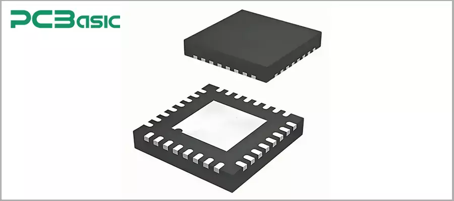
The QFN package has a very compact structure. Next, we will explain it from its internal and external structure.
The internal structure of QFN packaging mainly consists of a silicon chip and a substrate. The silicon chip is its core chip area. It is located at the center of the package and carries the core components of the integrated circuit, such as processors and RF chips. Chips are usually installed in plastic or ceramic casings.
The external structure design of the QFN package is very compact and efficient. Its shape is usually square or rectangular, and the external encapsulation is made of plastic or epoxy resin materials. The bottom of the QFN package is its most distinctive feature. It is composed of metal pads arranged along the four edges of the package, providing an electrical connection to the PCB circuit board. In addition, to enhance the heat dissipation effect of the QFN, there is a hot pad located at the center of the bottom of the package. This pad can effectively conduct heat from the chip to the PCB and then dissipate it through the PCB board. The presence of hot pads is a major advantage of QFN packaging, which can effectively lower the temperature and prevent overheating problems.
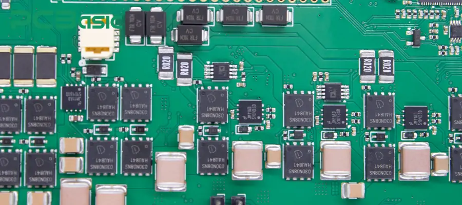
1. One of the greatest advantages of QFN packaging is its compact size. This feature makes it highly suitable for space-constrained applications, such as smartphones and wearable devices.
2. Superior thermal performance is also a major advantage of QFN packaging. The QFN package is equipped with exposed heat dissipation pads, which can dissipate heat more effectively. This feature makes it highly suitable for high-power applications, because it can prevent overheating and maintain stable performance.
3. The electrical path of QFN packaging is relatively short, featuring low inductance and excellent signal integrity. This is highly suitable for high-speed and high-frequency circuits.
4. When soldering QFN, visual inspection is very difficult as the pads are located at the bottom of the package. X-ray inspection technology is usually required to check the welding points.
QFN packaging is widely used in various fields. It is particularly common in scenarios where the size is compact, the performance is excellent and the heat dissipation efficiency is high. In consumer electronics such as smartphones, tablets and wearable devices, QFN is highly favored for its small size and excellent electrical performance. In the field of automotive electronics, QFN packaging is often applied to key components such as sensors and control units.
In addition, QFN packaging also plays a significant role in industrial electronics and communication equipment. It is often used in industrial control systems, communication modules and signal processing units. Because it not only saves space, but also has good thermal management capabilities and electrical performance.
The full name of QFP is quad flat package. It is an SMT packaging type that is widely used in various electronic products. Unlike QFN, the characteristic of QFP is that it extends outward curved pins (gull-wing-shaped pins) around the package body. These pins not only facilitate soldering and inspection, but also can reliably establish a connection with the PCB circuit board. QFP packaging is easy to operate, suitable for automated production and highly compatible, and is applicable to various types of integrated circuits.
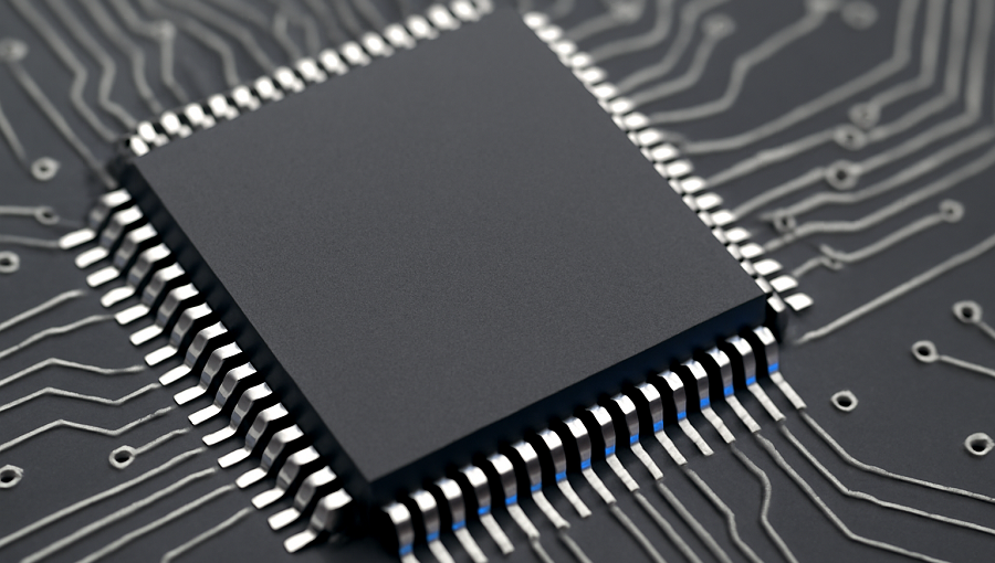
The structure of QFP can also be understood from two aspects: internal structure and external structure.
The interior of a QFP package is typically composed of silicon chips, Lead frames and packaging materials. The chip is installed on the lead frame and connected to the pins on all four sides through metal wires. The entire internal circuit will be encapsulated with plastic or ceramic materials to provide protection and mechanical strength.
The appearance of QFP packages is usually square or rectangular. The most notable external feature is its gull-wing-shaped pins. These pins extend from the four sides, first bending downward and then expanding outward. This design facilitates visual inspection of the welding condition and supports later rework. This exposed type of pin is very suitable for AOI inspection and is more convenient during maintenance.
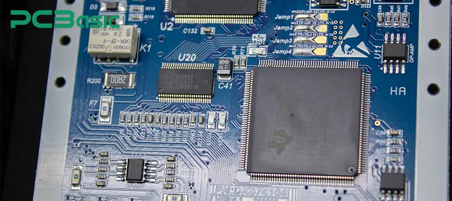
1. One of the major features of QFP compared with QFN is its strong pin visibility. Its external pins are prominently exposed, making it very convenient for soldering, inspection and rework.
2. QFP has a compact structure but is still slightly larger than QFN, supporting a medium to high number of pins (up to hundreds of pins).
3. QFP has good compatibility. This makes it highly suitable for multi-pin high-performance chips such as microcontrollers, FPGAs, and DSPS.
4. The heat dissipation capacity of QFP is moderate and its thermal efficiency is not as high as that of QFN. However, some of its enhanced versions (such as HTQFP) are equipped with heat dissipation pads and have a certain heat dissipation capacity.
5. QFP has pins on all four sides, making it highly suitable for complex circuit designs that require a large number of pins.
QFP packaging is widely used in multiple fields such as consumer electronics, industrial control systems, automotive electronics, and embedded devices. In consumer electronics such as televisions, game consoles, and routers, QFP is often used in microcontrollers and signal processing chips. In automotive electronics, it is used in key components such as control modules, display drivers, and power control.
In addition, in industrial control equipment and communication systems, QFP packaging is popular due to its ease of detection, numerous pins, and mature production process.
|
Aspect |
QFN Package |
QFP Package |
|
Package Structure |
No leads, bottom pad connections |
Gull-wing leads on all four sides |
|
Size |
Smaller, space-saving |
Larger footprint, easier routing |
|
Pin Configuration |
Medium pin count, hard to inspect |
High pin count, easy to inspect |
|
Electrical/Thermal |
Good heat dissipation, short paths |
Average thermal, stable signals |
|
Assembly & Inspection |
High precision, hard to rework |
Easy placement, supports visual inspection |
|
Applications |
High-frequency, compact devices |
Controllers, logic, large ICs |
|
Cost |
Less material, low volume cost |
Mature process, slightly higher cost |
As can be seen from the above quick comparison table, there are obvious differences between QFN and QFP packages in several key aspects. Next, we will conduct a detailed analysis item by item.
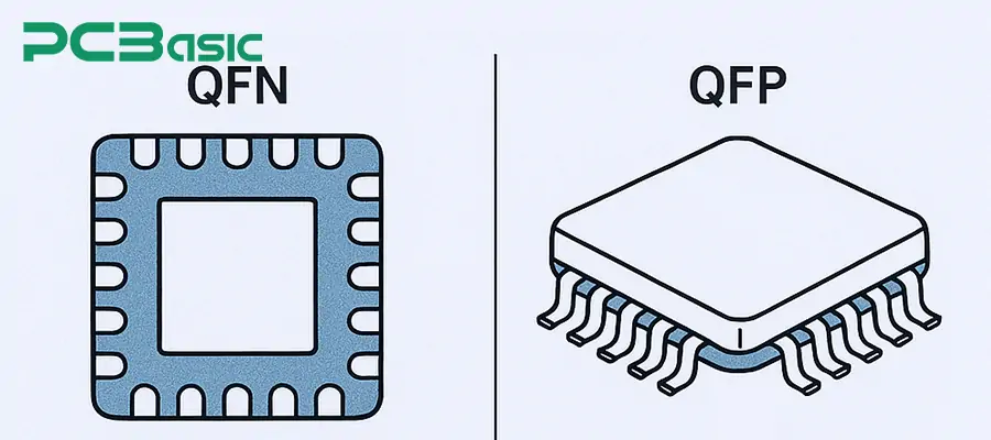
The most distinctive feature of the QFN package (Quad Flat No-Lead) is that it has no pins on the side. All electrical connections are achieved through the metal pads at the bottom of the package. In contrast, the QFP uses gull-wing leads on all four sides. The pins extend out of the package body, facilitating soldering and inspection.
This structural difference will directly affect the subsequent inspection, assembly process and design layout.
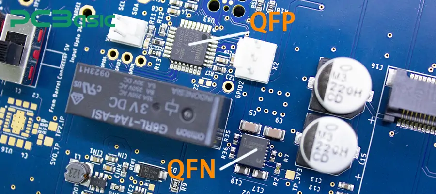
In terms of size, QFN packaging can significantly save circuit board space as it has no external pins. Therefore, it is often used in space-constrained designs, such as wearable devices. However, QFP, due to exposed pins, has a larger overall package volume and occupies more PCB board area. However, this structure provides more space for routing design and is suitable for occasions where the PCB area is spacious.
If there is a high requirement for PCB space, QFN is a better choice. If convenience in wiring and cabling is pursued, QFP is more suitable.
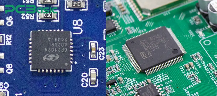
QFN packages typically support a moderate number of pins (commonly 16 to 80 pins). Its pads are hidden at the bottom and are difficult to inspect directly with the naked eye. The QFP package supports a higher number of pins, often exceeding 100 pins, and even reaching over 200. The pins are exposed, facilitating testing and inspection.
If the design requires the extraction of multiple signal or control ports, then choosing QFP is more advantageous. If the number of pins is not large, QFN saves more space.
QFN has a shorter electrical path, which can significantly reduce parasitic inductance and enhance signal integrity. Meanwhile, its bottom often features large exposed heat dissipation pads, which can directly conduct the heat from the chip to the PCB, effectively reducing the temperature. However, the QFP pin is relatively long and may introduce signal loss in high-frequency circuits, so it is not suitable for high-frequency circuits. Moreover, the heat dissipation capacity of QFP is average.
QFN packaging has relatively high precision requirements in surface mount assembly. Because its pads are at the bottom and the solder joints are not visible, X-ray inspection equipment is needed to confirm the welding quality. This also makes it difficult to repair when soldering fails. However, QFP is different. We can directly observe its pins, making the soldering process easier to control and more convenient for maintenance.
QFN is often used in products with high requirements for volume, electrical performance and heat dissipation. For example, RF modules, PMICs, wearable devices and portable sensors, Internet of Things communication chips, etc. QFN has also given rise to various variants (such as TQFN, VQFN, etc.) to meet different package sizes and heat dissipation requirements.
QFP is more suitable for MCU, FPGA/DSP chips, industrial logic controllers, and automotive electronic control systems.
In mass production, QFN packaging has a lower cost. Because it has a simple packaging structure, less material, small volume and high processing efficiency.
Although the unit price of QFP packaging is slightly higher, it has a mature process, strong detectability and is easy to operate.
If you focus on material costs and space efficiency, QFN is better. If you need good process compatibility and ease of debugging, then QFP is more suitable.
QFN and QFP are two classic surface mount packages in modern electronic products. The two seem very similar, but in fact they are not the same. Choosing the right IC package is very important, so it is necessary to have a clear understanding of the differences between QFN and QFP. Both QFN and QFP have their own unique advantages. QFN can provide compact size and top-notch performance for dense high-frequency layouts. QFP, on the other hand, excels in the accessibility and ease of assembly of high-pin-count ICs.
Overall, the choice between QFN and QFP should be weighed based on specific needs. When choosing IC packaging, we need to consider multiple aspects including size limitations, thermal management, pin configuration, assembly complexity and cost control. This article elaborately introduces and explains the differences between QFN and QFP. By now, you should have a clear understanding of the differences between QFN and QFP.
 About PCBasic
Time is money in your projects – and PCBasic gets it. PCBasic is a PCB assembly company that delivers fast, flawless results every time. Our comprehensive PCB assembly services include expert engineering support at every step, ensuring top quality in every board. As a leading PCB assembly manufacturer, we provide a one-stop solution that streamlines your supply chain. Partner with our advanced PCB prototype factory for quick turnarounds and superior results you can trust.

Assembly Enquiry
Instant Quote
Phone contact

+86-755-27218592
In addition, we've prepared a Help Center. We recommend checking it before reaching out, as your question and its answer may already be clearly explained there.
Wechat Support

In addition, we've prepared a Help Center. We recommend checking it before reaching out, as your question and its answer may already be clearly explained there.
WhatsApp Support

In addition, we've prepared a Help Center. We recommend checking it before reaching out, as your question and its answer may already be clearly explained there.