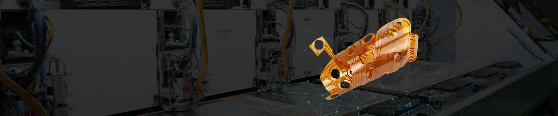
Flexible
printed circuit boards bend to fit curved and tight spaces. They use thin
layers of copper on a flexible film that lets engineers build smaller devices.
You can find them inside cameras, smartphones, and medical tools. The bend and
fold give new layout options and allow them to carry signals with high
reliability.
Flexible PCBs help cut space and weight
in devices. Designers can create gear that looks slim and light while wearable
gadgets gain comfort and strength. Makers can reduce assembly steps, thus
saving time on production lines. Flexible boards also stand up to motion and
stress in daily use. A wide variety of gadgets, including electric cars,
drones, and smart homes, use this technology. This growth shapes many new tools
for you.
Read on as we look at main types of
flexible PCBs, the structure, and their pros and cons. We will also compare
them with the more popular rigid PCBs and why you should consider the flexible
PCBs.
What is a Flexible PCB?
A flexible printed circuit board (PCB) is
a thin electronic board built on a bendable film. It holds copper traces that
carry power and signals across the board. The base film may twist or wrap
around parts. You can also shape it to fit tight or curved spaces. This freedom
makes it ideal when a flat board will not do.
Rigid PCBs sit on a hard, flat substrate
that resist bending and hold shape under stress. Flexible PCBs on the other
hand bend and flex with motion or tight fits. You can fold them inside compact
devices, therefore saving connectors and cables. It also cuts weight and
assembly steps. This design change makes many new layouts possible for you.
Flexible boards use films like polyimide
or polyester as substrates. Copper foil bonds to that film with special
adhesive and a coverlay protects traces while keeping flex. You may see
stiffeners added to hold parts and also find cover films for insulation and
strength. Layer count and thickness vary by use to balance flex and durability.
You find flexible PCBs in cameras,
phones, wearables, and sensors. They fit inside medical scanners, smart
glasses, and drones. Automakers use them in dashboards and sensors while
spacecraft and satellites rely on their light weight and bend. Flexible boards
are also very essential in robots that move.
Types of Flexible Circuit Boards
There are many types of flexible PCBs
that are used for different electrical components and devices. Here is a closer
look at some of them.
Single-sided Flex PCB
A single-sided flex PCB places copper
traces on one side of a thin film. The polyimide film functions as a signal
carrier when it bends through small spaces. A coverlay provides protection to
the traces and marks which serve as folding points. This layout design produces
a thin board with affordable costs for basic electronic pathways.
Engineers usually apply single-sided flex
boards for sensor ribbons and LED strips as well as basic signal links. The
board will experience one bending motion during manufacturing or remain flat. A
single cut in the harnesses and cables reduces both the amount of space
required and system weight. The single copper layer also allows fabrication
companies to maintain low production costs while keeping manufacturing
processes straightforward for short production runs.
The designcannot support complex wiring without additional jumpers. The entire
trace path receives your meticulous planning, which eliminates any possibility
of crossovers. Additional connections require either jumpers or external wires.
The addition of stiffeners leads to increased board thickness because they
serve as connectors or part mounting elements.
Double-sided Flex PCB
A double-sided flex PCB holds copper on
both sides of its film. Through-holes and microvias connect the various layers
of the board. The additional routing capabilities increase within the same
dimensional area. Each side of the flex PCB features protective coverlays which
also strengthen areas prone to bending. The board maintains its thin profile
when dealing with average complexity levels and signal densities.
Double-sided flex PCBs appear inside
barcode scanners and camera cables, as well as LED backlights. The additional
layer enables better performance by dividing power from data lines. Fabrication
processes that include drilling and plating operations drive manufacturing
expenses above the levels of single-sided construction. The flexibility in part
placement and critical net routing shows gains to designers.
The process of routing at bend zones
requires thorough planning to prevent vias from cracking. The fabrication
process requires you to position vias in areas that avoid curved sections while
employing reinforced openings in the coverlay. The fabricator rules determine
trace dimensions for maintaining dependability during bending operations. The
established rules enable you to achieve high-density while maintaining
long-term reliability in wearable and foldable systems.
Multi-layered Flex PCB
The multi-layered flex PCB combines three
or more copper layers inside flexible films. The internal copper layers
incorporate power planes and ground planes which function to reduce noise.
Connection of layers happens through blind or buried microvias to minimize
space requirements. A layer of coverlay bonds across the stack which protects
all copper layers from flex wear.
The high-speed circuit designs, along
with RF modules and compact camera connections, benefit from this specific type
of flex PCB. A thin, flexible package contains layers for power supply and
grounding while transmitting signals. Better signal integrity and EMI control
are obtained through design trade-offs with increased costs. The fabrication
process needs exact alignment, specific lamination pressures, and controlled
heat treatment for each adhesive layer.
Early determination of layer counts
proves vital because additional layers create both thickness and additional
etching processes. Critical nets need to be mapped onto inner layers to achieve
protection during movement. The number of layers in the stack-up determines the
bend radius limitations, which designers must consider when matching their
design requirements to these constraints. The balance between reliability and
flexibility can be maintained throughout the board.
Flex PCB
Any electronic circuit that uses flexible
substrate film to construct its design qualifies as a flex PCB. A flex PCB
design includes basic one-layer configurations along with intricate multi-layer
construction types. The selection of materials and copper thickness depends on
the expected number of flexes. Static flex boards experience single bending,
while dynamic flex boards need to handle continuous bending movements.
Static flex boards specifically serve to
support camera and phone assembly folds. The process requires you to bend them
and then keep them in their new position. Moving joints and folding displays
require dynamic flex boards to operate inside them. Special designs must be
implemented for copper stress relief and neutral bend lines. Your board design
will endure multiple thousands of bending cycles without sustaining any damage.
Flex PCB selection allows you to find a
balance between motion requirements and product expenses. The cost of
single-use bends remains lower than the expense of dynamic builds throughout
design and production. The selection of appropriate film and coverlay style and
trace shape depends on your motion profile and budget requirements and you work
with your fabricator to make these choices.
Flex with stiffener(s)
Rigid pads attached to flex PCBs function
as stiffeners which support heavy parts and connectors. The stiffener materials
consist of FR4 and polyimide and thin metal sheets. Bonds are used to attach
stiffeners at locations requiring flat mounting or extra strength. A
combination of flexible and rigid zones in the film design enables connector
attachment without causing damage to the film material.
The design process requires designers to
install stiffeners beneath board edges while also positioning them beneath
connector pads and test points. Board gets cut into shape with small openings
maintained to ensure nearby bending remains possible. The adhesive layers
provide secure attachment of stiffeners while preventing the buildup of
delamination or bumps. Transitions between stiffeners are covered with coverlay
to achieve smooth bending.
The introduction of stiffeners affects
board thickness at specific areas thus you need to verify assembly tool
accessibility. You need to modify both solder paste stencils and pick-and-place
equipment settings. The additional setup process guarantees parts maintain
proper alignment and solder joints maintain their strength despite movements in
the surrounding flex film.
Rigid-flex PCB
A rigid-flex PCB combines rigid board
sections and flex sections in one part. The fabrication process involves
placing flexible films between rigid layers before bonding all the layers
together. The hybrid design eliminates cable requirements because rigid islands
use flex bridges to connect with each other. The board maintains its strength
in specific areas but develops flexibility in other sections.
Rigid-flex PCB applications exist in
aerospace and medical implants and military equipment. These boards function
effectively in demanding environments which require different levels of
stiffness. The board contains rigid parts which support heavy components and
flex sections that create cable-like structures or folding capabilities.
Fabrication requires exact layer bonding and controlled laminating and precise
alignment of copper areas.
The design process of rigid-flex begins
with establishing mechanical fits and determining bend profiles from the start.
Your design determines the flat regions and the areas that need to fold. Your
CAD tool needs to support the design of both rigid and flexible stack-up
features. The process of careful planning results in a single assembly that
reduces weight and space requirements and simplifies assembly steps.
Structure of Flexible PCBs
The construction of a flexible board
resembles a thin sandwich structure with bendable properties. The main
component of this system is a flexible substrate material. Films act as a base
where copper foil attaches to create necessary circuits.
The adhesive layers function as binding
materials to hold the circuit components in position during bending operations.
The copper traces receive protection from wear and moisture through the
application of a top coverlay layer.
How Much Can You Bend a PCB?
The bend radius determines the maximum
curvature of flex boards. The standard measurement for bending flexibility
equals ten times the thickness of the board. A 1 mm radius serves as the
minimum requirement for bending a 0.1-mm-thick board without causing any
damage. A single bend works with five times thickness, yet this could lead to
board fractures.
Material choices affect flexibility. The
material polyimide maintains its strength properties when heated and supports
many flexible cycles. Polyester material serves best when designing static
bends. Copper thickness also matters. The bending strength of thin copper
increases while the required stress decreases.
Role of Stiffener in Flex PCB Design
Stiffeners serve to maintain flatness and
stability of component pads. The stiffeners find their position under
connectors and ICs and test points. Solder joints tend to crack when stiffeners
are absent during flexing. You should use heat-resistant adhesive to connect
stiffeners. The component stays fixed in position while board movement remains
blocked.
The most frequently used stiffener
materials consist of FR4 and polyimide and aluminum. FR4 offers a low-cost,
rigid base. Polyimide stiffeners match substrate flexibility. Aluminum serves
as a strong material for connectors that need additional structural support.
Stiffeners need shaping before bending while you maintain reveal edges for the
process. The placement of stiffeners occurs either beneath components or at the
board edges to direct assembly processes.
The addition of stiffeners affects the
thickness of specific board areas. Before assembly you need to account for both
height requirements and assembly gap allowances. Environmental stress is
protected by applying tape or coverlay to the edges of stiffeners. The
placement of stiffener edges under tape or coverlay ensures both routing
quality and protects the film from peeling at stiffener-flex section junctions.
Designing Tips for Flexible Printed Circuit Boards
Plan trace width and spacing early in the
layout. Wider traces carry more current but add stiffness. Narrower traces let
you bend tighter but limit current. Use consistent spacing to prevent shorting
under flex. Keep the minimum values within your fabricator's capabilities.
Map out bend areas and keep sensitive
nets away. Place bend lines where the board will curve gently. Avoid placing
vias on fold zones. Add relief patterns like dog-bone shapes at trace ends.
That spreads stress and prevents cracks when the board flexes.
Place components outside bend zones when
you can. Use surface-mount parts with low profiles. If you must put parts on a
bend zone, use flexible connectors or zero-insertion-force sockets. Route
high-speed or high-precision nets on stable sections to cut signal distortion
from flex motion.
Choose CAD tools that handle flex
stack-up and bend simulation. Many PCB tools let you draw neutral bend lines
and visualize copper stress. Define layer buildup with substrate, adhesive,
copper, and coverlay. Export bend data to mechanical CAD for enclosure design.
That workflow ensures you catch fit or collision issues early.
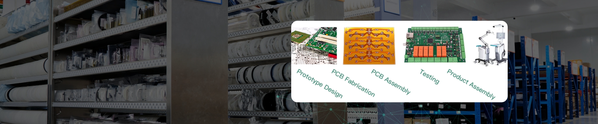
About PCBasic
Time is money in your projects – and PCBasic gets it. PCBasic is a PCB assembly company that delivers fast, flawless results every time. Our comprehensive PCB assembly services include expert engineering support at every step, ensuring top quality in every board. As a leading PCB assembly manufacturer, we provide a one-stop solution that streamlines your supply chain. Partner with our advanced PCB prototype factory for quick turnarounds and superior results you can trust.
Advantages of Flexible PCBs
Flexible PCBs come with many advantages
that let you design tight layouts with few parts. Here are the main pros.
• It saves space by
folding the board into tight spots.
• They cut the weight
in your device by using thin films.
• You remove extra
cables and connectors from your design.
• They lower assembly
steps and speed up production.
• They last longer in moving
parts with boards that bend.
• You cut shipping costs with a lighter final product.
Shortcomings of Flexible PCBs
Although Flex PCBs come with many
advantages, there are a few shortcomings that come with them. Here are some.
• You may pay more in
material and special processing fees.
• They need careful
handling and custom assembly fixtures.
• They limit how much
load you place on bend areas.
• You must add
stiffeners for heavy connectors or parts.
• They require testing and inspection to catch flex damage early.
Flex PCB vs. Rigid-flex PCB
The manufacturing methods of flex and
rigid-flex PCBs differ although they serve the same functional requirements.
The following table illustrates major distinctions between flex and rigid-flex
PCBs.
Feature
Flex PCB
Rigid-Flex PCB
Structure
Single bendable film
with copper traces
A mix of rigid boards
and flex layers in one board
Bend Areas
All sections bend
(static or dynamic)
Only flex sections bend
and rigid parts stay flat
Component Mounting
Parts sit on flexible
film or use stiffeners
Parts mount on rigid
islands; flex links connect islands
Assembly Steps
Needs connectors or
solder joints
Fewer external
connectors but more layer-bonding steps
Flex PCB Prototype Fabrication Services from PCBasic
The quick-turn flex PCB prototype
fabrication service of PCBasic handles any level of prototype complexity. You
can send your Gerber files and stack-up specifications using our online
platform. Design review from our engineers provides advice about bend radius as
well as trace width features alongside coverlay passage dimensions. The
communication between you and the manufacturer happens through real-time email
and chat services.
PCBasic uses precision laser cutters to
mill your prototype before adding copper foil to polyimide films through
plotting processes. We follow your requirements to bond coverlay materials and
stiffeners. The assembly house within our company performs part soldering
operations while conducting functional tests through flex cycle procedures. The
report includes photos together with test logs and complete documentation.
Conclusion
Flexible PCB technology uncovers fresh
product designs through minimized space usage and reduced weight requirements
and simplified assembly procedures. The selection includes single-sided boards
and multi-layer and rigid-flex designs depending on your project requirements.
Reliability under motion becomes possible through careful planning of materials
and traces and bending considerations.
The expertise and rapid prototype
creation and production pathway which fabricators such as PCBasic offer their
customers. Using the appropriate flex board type enables you to develop slim
dynamic devices efficiently and with assurance.
We use cookies to enhance your experience, analyze traffic, and provide personalized content. By clicking “Accept Cookies”, you agree to our Cookie and Privacy Policy.
Manage Cookie Preferences
We use cookies to enhance your browsing experience. Please review the details of each cookie category below and choose your preferences.
Strictly Necessary Cookies
These cookies are essential for the website to function properly and cannot be disabled. They are typically set in response to actions you take, such as logging in or adding items to your shopping cart.
Performance Cookies
These cookies help us understand how visitors interact with our website by collecting information about traffic and usage. This allows us to measure and improve the website’s performance.
Targeting/Advertising Cookies
These cookies are used to deliver
advertisements relevant to you and your interests. They may also limit the number of times you see an
advertisement and help measure the effectiveness of advertising campaigns.
In addition, we've prepared a Help Center.
We recommend checking it before reaching out, as your question and its
answer may already be clearly explained there.
✖
Wechat Support
In addition, we've prepared a Help Center.
We recommend checking it before reaching out, as your question and its
answer may already be clearly explained there.
✖
WhatsApp Support
In addition, we've prepared a Help Center.
We recommend checking it before reaching out, as your question and its
answer may already be clearly explained there.


 About PCBasic


