Global high-mix volume high-speed PCBA manufacturer
9:00 -18:00, Mon. - Fri. (GMT+8)
9:00 -12:00, Sat. (GMT+8)
(Except Chinese public holidays)
Global high-mix volume high-speed PCBA manufacturer
9:00 -18:00, Mon. - Fri. (GMT+8)
9:00 -12:00, Sat. (GMT+8)
(Except Chinese public holidays)
HomePage > Blog > Knowledge Base > Flex PCB Prototyping: From Design Guidelines to Production
In the development of electronic products, innovation no longer solely depends on product performance; it also highly depends on form factor, reliability, and speed to market. With the continuous development of equipment towards miniaturization, lightweighting and complex structures, the flex PCB prototype has become an indispensable part of the engineering development process.
The core value of a flex PCB prototype lies in its ability to conduct comprehensive verification of electrical performance, reliability of the bending area, material selection, and assembly feasibility before mass production. It is a crucial stage for the smooth mass production of the product. This pre-verification method can significantly reduce the risk of rework, shorten the development cycle, and enhance the overall success rate of the project.
This article will focus on the flex PCB prototype and systematically introduce the complete technical path from design to pre-production validation, including its core advantages, typical application scenarios, different types of prototype structures, common flex PCB materials and surface finish solutions, as well as manufacturability-oriented design for flex PCB manufacturing, and an introduction to the support methods of PCBasic’s flex PCB prototyping capabilities in real-world engineering projects.
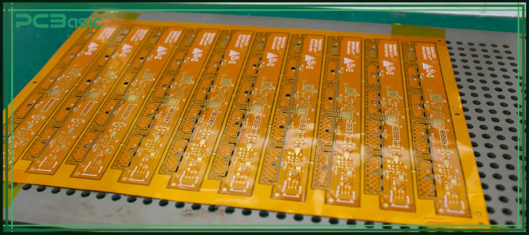
A flex PCB prototype is a functional flexible circuit board made in the early stage of a project to verify the feasibility of the design plan. It is usually manufactured based on flexible substrates, with polyimide being the most common material.
Unlike rigid PCBs, flex circuit boards need to withstand bending, folding or twisting during operation while still maintaining stable electrical connections.
Depending on the design complexity, flex PCB prototypes can adopt single-sided, double-sided, multilayer or rigid-flex combined structures, and can include through-holes, blind holes or microvias. The main function of these flex PCB prototypes is to verify key risk points before mass production, including:
• Whether the board can bend safely within the required bend radius
• Whether electrical connections remain stable under mechanical stress
• Whether the layout and materials are suitable for flex PCB assembly
• Whether the board can withstand heat, vibration, and environmental conditions
For engineering teams that need to collaborate with flex circuit board manufacturers, making a flex PCB prototype is a key step to identify problems in advance, reduce repeated modifications, and improve the success rate of flex PCB manufacturing.
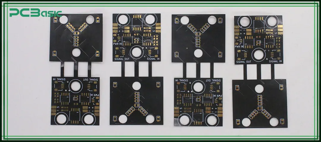
Flex PCB designs can complete electrical connections within a limited space, reducing the use of wiring harnesses and connectors.
Flex circuit structures can withstand repeated bending, vibration and dynamic movement without being easily damaged.
Through flex PCB prototyping, signal path designs can be verified earlier to ensure proper routing and electrical performance.
Flex PCB assembly typically involves fewer assembly steps and a simpler interconnection structure. The reduction in the number of connection points makes the overall reliability of the system higher.
The application of flex PCB prototypes almost covers all advanced electronic fields:
|
Industry |
Typical Products |
Role of the flex PCB prototype |
|
Consumer Electronics |
Smartphones, tablets, cameras, and foldable devices |
Enables ultra-thin layouts, tight internal routing, and early validation of bending performance and assembly fit |
|
Automotive Electronics |
Dashboards, lighting modules, sensors, and ADAS systems |
Verifies reliability under vibration, temperature changes, and long-term mechanical stress |
|
Medical Devices |
Imaging systems, diagnostic equipment, wearable monitors |
Validates compact design, electrical stability, and suitability for sensitive or biocompatible applications |
|
Aerospace & Defense |
Avionics, control systems, communication modules |
Confirms resistance to shock, extreme temperatures, and harsh operating environments |
|
Industrial & Wearables |
Robotics, IoT devices, wearable electronics |
Tests durability under repeated movement and ensures stable signal performance in dynamic use |
According to different specific application requirements, flex PCB prototypes can be structurally classified into several structural types.
The single-sided flex PCB prototype only arranges a single layer of copper foil structure on the flexible substrate, with an overall thin thickness and high flexibility.
The double-sided flex PCB prototype achieves electrical connection between the top and bottom copper layers through plated through-holes, which can support more complex routing requirements.
The multilayer flex PCB prototype adopts three or more conductive layers, which can incorporate blind vias and buried vias for high-density signal interconnection.
The rigid-flex prototype contains both rigid section and flexible interconnect areas in the same circuit.
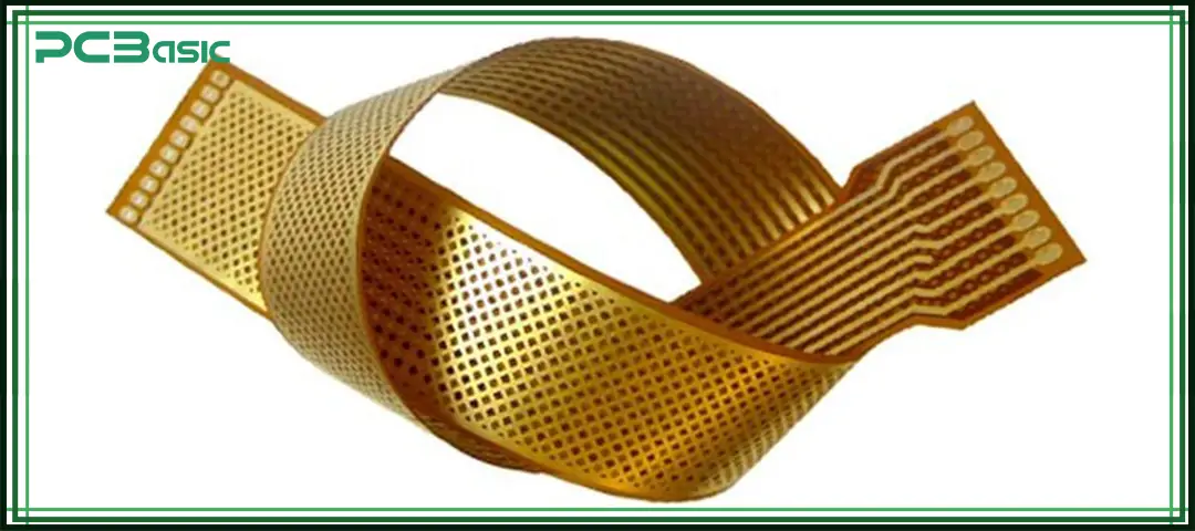
The choice of surface finish directly affects the solderability, durability and long-term reliability of the flex PCB prototype.
ENIG (Electroless Nickel Immersion Gold)
• Provides a flat and uniform surface
• Offers strong oxidation resistance
• Is the most commonly used surface finish in flex PCB fabrication
Other optional surface finishes
• Immersion Silver
• Immersion Tin
• OSP
• Electrolytic Gold
The design of the stacked structure needs to strike a balance among multiple factors to ensure the stability of the flexible PCB prototype during bending and use.
Copper thickness, dielectric layers, and adhesive systems must be properly matched.
Proper stack-up planning helps ensure:
• Consistent bending performance
• Stable behavior from flex PCB prototyping through volume production
• Improved manufacturability and overall reliability
Time is money in your projects – and PCBasic gets it. PCBasic is a PCB assembly company that delivers fast, flawless results every time. Our comprehensive PCB assembly services include expert engineering support at every step, ensuring top quality in every board. As a leading PCB assembly manufacturer, we provide a one-stop solution that streamlines your supply chain. Partner with our advanced PCB prototype factory for quick turnarounds and superior results you can trust.
If manufacturability is not fully considered when designing a flex PCB prototype, problems are often exposed in the flex PCB fabrication or flex PCB assembly stage, and may even lead to prototype failure.
First of all, the bending areas on the circuit board must be clearly defined. All components, vias and reinforcement structures should be avoided from being placed in the bending area; otherwise, mechanical stress is likely to occur during bending or repeated use, leading to cracking or functional failure.
In terms of wiring design, rounded traces should be adopted as much as possible to avoid sharp corner structures, so as to reduce copper fatigue during bending.
The bending radius is a key parameter that cannot be ignored in the prototyping of flex PCB. For dynamic applications that require repeated bending, the minimum bending radius should typically be no less than 10 to 12 times the total thickness of the material. Adding stiffeners to the connector or device mounting area helps improve the stability and reliability of flex PCB assembly.
Communicating with flex circuit board manufacturers as early as possible during the design stage can identify potential manufacturing risks in advance, significantly increase the probability of the first-time success of the flex PCB prototype, and reduce subsequent modifications and rework.
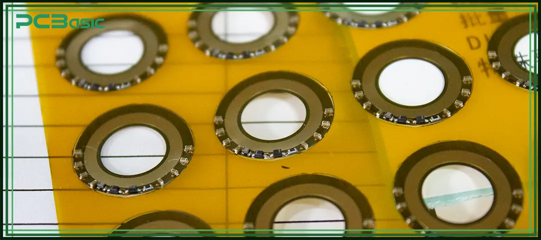
To ensure the reliability of the product before mass production, the flex PCB prototype must go through a complete and systematic testing and inspection process.
• Verifies electrical continuity and isolation
• Confirms that all signal paths function correctly
• Helps identify opens, shorts, and leakage issues early
• Ensures controlled impedance meets design requirements
• Reduces signal loss, noise, and EMI risks
• Critical for high-speed and high-density flex PCB designs
• Evaluates bend life and resistance to mechanical fatigue
• Simulates repeated bending and dynamic movement
• Confirms long-term reliability in real operating conditions
• Confirms accurate layer alignment
• Verifies plating thickness and via quality
• Detects hidden structural defects within the flex PCB stack-up
• IPC-6013 for flexible circuit board qualification
• IPC-A-610 for assembly workmanship standards
• ISO quality management systems guiding manufacturing and inspection
Through structured testing and compliance with recognized standards, it can be verified that the flexible PCB prototype can operate reliably under actual electrical, mechanical and environmental conditions.
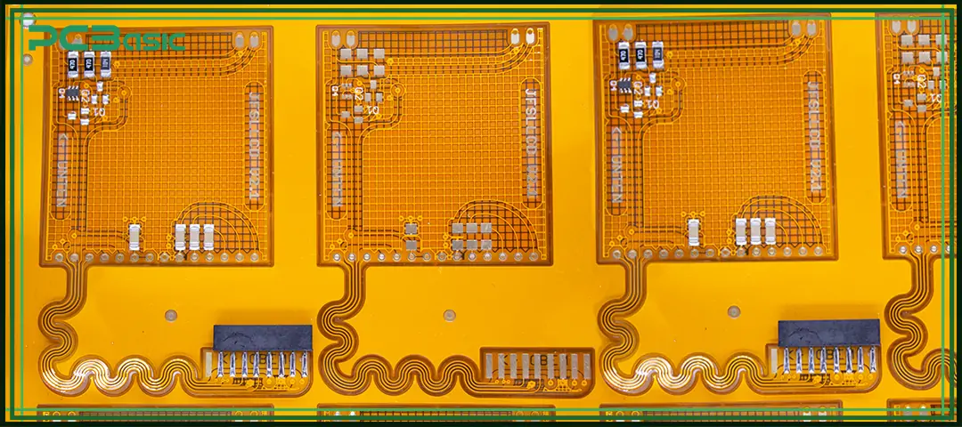
As an experienced flex PCB manufacturer, PCBasic provides complete flex PCB prototyping services focused on speed, reliability, and smooth transition to production.
PCBasic supports single-sided, double-sided, multilayer, and rigid-flex PCB prototypes, covering a wide range of flex PCB material, surface finishes, and stack-up options. With efficient, quick-turn flex PCB processes, prototypes can be delivered fast while maintaining stable quality.
From flex PCB fabrication to flex PCB assembly and full flex PCBA, PCBasic combines engineering review, design-for-manufacturability checks, functional testing, and production planning into one workflow. This ensures that every flex PCB prototype is not only electrically functional, but also ready for volume flex PCB manufacturing.
By combining solid technical support with fast response times, PCBasic helps customers move confidently from flex PCB prototyping to mass production with fewer risks and fewer revisions.
A successful flex PCB prototype is far more than just an early sample for verification; it is the foundation for building reliable and scalable electronic products. By aligning design rules, material selection, manufacturing constraints, and testing standards simultaneously during the design phase, flex PCB prototyping can effectively reduce project risks, accelerate development progress, and enhance the quality of the final product.
Whether it's wearable devices, automotive electronics, medical equipment, or aerospace systems, collaborating with an experienced flex circuit manufacturer can ensure that your flex PCB prototype operates as expected and smoothly transitions to the stage of flex PCB manufacturing.
When strategies, tools and engineering experience are well-matched, "flex PCB prototyping" will become a key force driving product innovation rather than a bottleneck in the development process.

Assembly Enquiry
Instant Quote
Phone contact

+86-755-27218592
In addition, we've prepared a Help Center. We recommend checking it before reaching out, as your question and its answer may already be clearly explained there.
Wechat Support

In addition, we've prepared a Help Center. We recommend checking it before reaching out, as your question and its answer may already be clearly explained there.
WhatsApp Support

In addition, we've prepared a Help Center. We recommend checking it before reaching out, as your question and its answer may already be clearly explained there.