Global high-mix volume high-speed PCBA manufacturer
9:00 -18:00, Mon. - Fri. (GMT+8)
9:00 -12:00, Sat. (GMT+8)
(Except Chinese public holidays)
Global high-mix volume high-speed PCBA manufacturer
9:00 -18:00, Mon. - Fri. (GMT+8)
9:00 -12:00, Sat. (GMT+8)
(Except Chinese public holidays)
HomePage > Blog > Knowledge Base > High-Frequency PCB Materials and Signal Integrity Control
The operating frequency and data rate of electronic systems are constantly increasing, and the impact of high-frequency PCB design on overall electrical performance is also magnified. In many modern applications, such as 5G communication, automotive radar, RF modules, and industrial electronics, the stability and consistency of signal transmission are indispensable. Under high-frequency conditions, traditional PCB design is difficult to meet the actual requirements. This places higher demands on system reliability.
However, the material properties of PCBs and signal integrity are the key factors determining the performance of high-frequency circuits. In this article, we will discuss the issue of signal integrity from the perspective of high-frequency PCB materials.
In high-frequency PCB design, signal integrity refers to the ability of an electrical signal to maintain its original form during transmission from the sender to the receiver without significant distortion, excessive attenuation, or timing errors. Simply put, good signal integrity means that the signal remains close to its initial state when it reaches the terminal.
As the working frequency and data rate continue to increase, the signal transmission method on PCBs has also changed. In high-frequency circuit boards, signals are no longer merely simple voltage changes but propagate in the form of electromagnetic waves along traces, reference planes, vias, and connectors. Therefore, in high-frequency PCBs, each signal trace should be regarded as a transmission line. Its electrical characteristics directly affect signal integrity.

Why is signal integrity so crucial in high-frequency PCB design?
This is because, in low-frequency circuits, minor changes in the width of the traces or material parameters usually do not have a significant impact on signal integrity. However, in high-frequency or high-speed PCB designs, even very small discontinuities can cause serious signal problems.
In high-frequency circuits, good signal integrity helps to ensure:
The signal waveform is stable and predictable.
The timing and synchronization are accurate.
Low bit error rate in high-speed digital systems.
Performance consistency in RF and microwave circuits.
If signal integrity control is inadequate, high-frequency PCBs may experience unstable functionality, reduced reliability, and even fail to pass electrical or EMC-related tests.
In high-frequency PCBs, the common signal integrity issues include:
|
Issue Type |
Root Cause |
Impact on Signals |
|
Impedance Mismatch & Signal Reflection |
Characteristic impedance of PCB traces does not match the source or load impedance |
Waveform distortion, ringing, overshoot |
|
Insertion Loss & Dielectric Loss |
Energy loss caused by dielectric loss (Df) and conductor loss |
Reduced signal amplitude, limited transmission distance |
|
Crosstalk |
Electromagnetic coupling between adjacent traces |
Introduced noise and jitter, reduced signal stability |
|
Timing Skew & Jitter |
Inconsistent trace length, routing structure, or dielectric constant (Dk) |
Reduced timing margin, increased bit error rate |
|
Electromagnetic Interference (EMI) |
Poor return paths and radiation of high-frequency energy |
Interference with nearby circuits, compliance risks |
Signal integrity is not merely dependent on the wiring itself; it is a system-level issue and is also influenced by the following factors:
Dielectric constant (Dk) and loss factor (Df) of PCB materials
Stack-up structure and reference plane design
Via structure and interlayer transition method
Connector and device interface characteristics
Any change in any of the components will have an impact on the overall signal integrity.
When choosing high-frequency PCB materials, we can make a judgment by considering several key electrical parameters that directly affect signal integrity. Among the numerous parameters of high-frequency PCBs, dielectric properties, loss characteristics, control of dielectric thickness, and material stability are the most crucial.
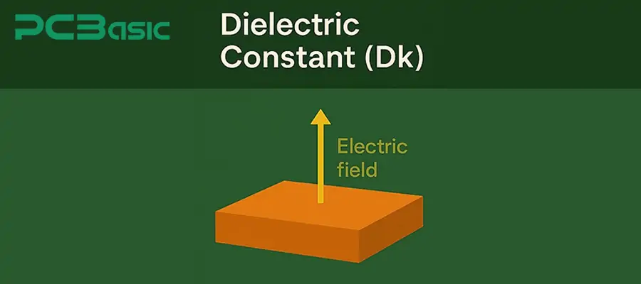
The dielectric constant (Dk) describes the ability of PCB materials to slow down the signal propagation speed relative to vacuum. In high-frequency PCB design, Dk directly affects the signal propagation speed, impedance calculation, and phase characteristics. Generally, a lower Dk helps signals propagate faster on the traces, thereby reducing propagation delay and improving timing accuracy.
If Dk is unstable or poorly controlled, it can easily lead to impedance fluctuations, thereby causing signal reflection, waveform distortion and timing errors. High-frequency PCB materials usually have stricter control over Dk than ordinary FR-4.
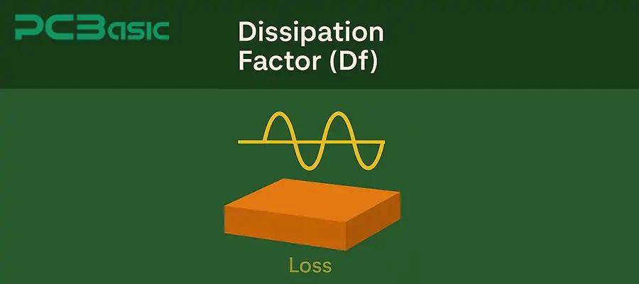
The loss factor (Df), also known as the tangent of the loss angle, is used to measure the proportion of electromagnetic signals that are converted into heat energy when propagating in dielectric materials. Dielectric loss is one of the main sources of signal attenuation in high-frequency PCBs. As the frequency increases, even a small difference in Df will be amplified in long traces or high-speed signal channels, significantly affecting insertion loss.
Regarding Df, the following points need to be focused on:
The lower the Df, the smaller the insertion loss.
This is particularly crucial for long-distance routing and high-speed serial links.
It is almost an indispensable parameter in RF, microwave, and millimeter-wave PCB applications.
Compared with ordinary FR-4, high-frequency PCB materials usually have significantly lower Df values.
For high-frequency PCB design, the control of the dielectric thickness between the signal layer and the reference plane is crucial for maintaining a stable impedance. Even a very small change in thickness can cause a change in the characteristic impedance of the traces, leading to impedance mismatch and subsequently affecting signal integrity.
Therefore, in the production process of high-frequency PCB materials, stricter control of thickness tolerance is required to support precise impedance design. If the dielectric thickness is inconsistent, it may lead to:
The wiring impedance varies along the line.
There is an increase in signal reflection.
The consistency between different batches of PCBs decreases.
The copper-clad laminate (PCB) uses glass fiber as the reinforcing material, which may introduce the glass fiber weaving effect. Then, due to the uneven distribution of the glass fibers, the dielectric constant under the traces is prone to undergo local changes. In high-frequency applications, such changes may cause phase distortion and timing deviations. To mitigate this impact, high-frequency PCB materials typically employ:
Spread Glass
Optimized glass fiber weaving method
Other alternative reinforcing structures
These methods can improve the uniformity of Dk and reduce signal deviations.
Thermal stability and mechanical consistency also indirectly affect the integrity of the signal. During PCB assembly and actual usage, the materials need to undergo temperature changes, reflow soldering cycles, and long-term thermal stress. Therefore, high-frequency PCB materials should be able to maintain stability in the following aspects:
At different temperature conditions, the values of Dk and Df remain stable.
After undergoing multiple reflow soldering processes, the electrical performance does not show significant changes.
During long-term use, it maintains good mechanical integrity.
If stability cannot be maintained in the above aspects, the impedance and signal loss will change accordingly, thereby affecting the long-term reliability of high-frequency applications.
Next, let's take a look at several commonly used high-frequency PCB materials. These materials vary in terms of electrical performance, processing difficulty, cost, and applicable scenarios. The table below highlights their main characteristics and typical applications.
|
Material Type |
Electrical Characteristics |
Manufacturability & Cost |
Typical Applications |
|
PTFE-Based Materials |
Extremely low Dk and ultra-low Df; excellent performance at microwave and mmWave frequencies |
Requires specialized processing; higher manufacturing cost |
RF antennas, radar systems, satellite communication |
|
Hydrocarbon Ceramic Laminates |
Low Dk and low Df; stable electrical performance over a wide frequency range |
Better process compatibility than PTFE; moderate cost |
Automotive radar, 5G base stations, high-speed networking |
|
Modified Epoxy High-Frequency Materials |
Improved Dk and Df compared to standard FR-4 |
Cost-effective; compatible with standard PCB fabrication |
Mid-range high-speed digital PCBs |
|
Polyimide-Based Materials |
Stable Dk and Df at high temperatures; excellent thermal resistance |
Higher material cost; suitable for harsh environments |
Aerospace electronics, industrial control, automotive electronics |
The selection of PCB materials directly affects the performance of signal integrity. The signal behavior is influenced by the electrical properties of the copper-clad laminate. At high-frequency conditions, PCB materials are not merely the basic material for carrying copper traces. They actively affect the way signals propagate on the circuit board.
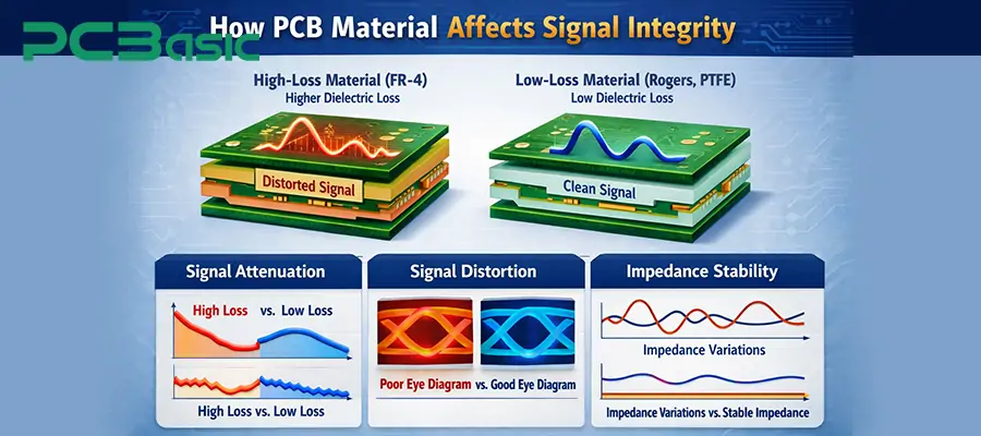
1. Impedance mismatch can lead to signal reflection. The characteristic impedance of PCB traces is mainly determined by two factors: the geometric structure of the traces (line width, spacing, copper thickness) and the dielectric properties of the PCB material, especially the Dk and the dielectric thickness.
When the Dk value is inconsistent throughout the board or there is a fluctuation in the dielectric thickness, impedance mismatch will occur. This mismatch will cause signal reflection, thereby reducing signal integrity.
2. The higher the frequency, the more obvious the signal attenuation problem will be. PCB materials with a higher loss factor (Df) will absorb more electromagnetic energy and convert it into heat, resulting in higher insertion loss.
In high-frequency and high-speed applications, excessive signal loss will:
Reduce signal amplitude
Narrow the eye diagram opening
Limit the effective transmission distance
Increase the risk of bit errors
Therefore, for high-frequency designs, we should use low-loss PCB materials to better maintain the signal strength.
3. The properties of PCB materials can affect the signal propagation delay, and the propagation delay is closely related to the dielectric constant. If the Dk changes with frequency, temperature, or location, the propagation delays of different signal paths will vary, thereby causing timing deviations.
4. The characteristics of PCB materials also affect the propagation and interaction of electromagnetic fields within the circuit board. When the material consistency is poor, unnecessary radiation and coupling between adjacent traces are likely to occur, leading to EMI and crosstalk problems.
Overall, the selection of PCB materials is one of the key factors for signal integrity control. Choosing the appropriate high-frequency PCB materials is the foundation for achieving high-performance and high-reliability signal integrity.
In high-speed and high-frequency PCB design, signal integrity is the result of the combined effect of multiple factors. To truly achieve good signal integrity, not only is it necessary to select the appropriate high-frequency PCB materials, but also it is necessary to consider the design rules, wiring methods, and manufacturing accuracy as a whole. Here are some tips that can help achieve good signal integrity.
Controlled impedance routing is one of the most fundamental and crucial signal integrity control methods in high-frequency PCB design. Under high-frequency conditions, transmission lines must maintain a predetermined characteristic impedance (such as 50Ω, 90Ω, or 100Ω), otherwise it is prone to cause signal reflection and waveform distortion.
Common impedance control measures include:
Based on the stack structure and the dielectric constant (Dk) of the materials, accurately calculate the trace width and spacing
Maintain the consistency of the dielectric thickness between the signal layer and the reference plane
Strictly control the manufacturing tolerances to keep the actual impedance within a controllable range
Impedance control does not only occur during the design stage. We usually also need to verify the rationality of the design through simulation methods, and during the PCB manufacturing process, confirm the final results through impedance testing.
In high-speed and high-frequency PCBs, differential signals are widely used to enhance the anti-interference capability and reduce EMI. However, if the differential traces are not designed properly, timing deviations and signal degradation problems may still occur.
The main optimization points of differential pair wiring are:
Carry out strict matching of wire lengths to minimize timing deviations
Maintain a stable wire spacing to maintain the differential impedance as specified in the design goals
Avoid asymmetric wiring, sharp turns, and frequent layer switching
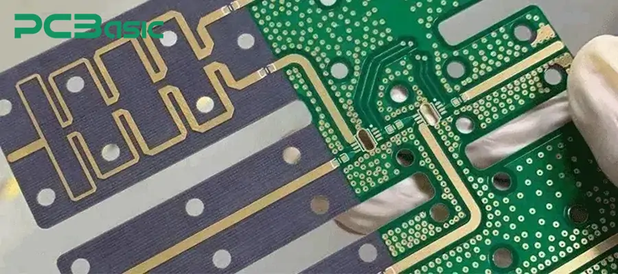
Vias will introduce impedance discontinuities and parasitic inductance in the signal path. Poorly designed via holes often lead to increased reflections, rising insertion loss, and increased EMI risks.
The commonly used methods for optimizing high-frequency vias include:
Using the back-drilling technique, remove the excess stubs of the vias
Employ microvias or buried vias to reduce parasitic inductance and parasitic capacitance
Model and optimize the key via transition structures for analysis
Reasonable control of the via structure can significantly improve the transmission quality and consistency of high-frequency signals.
A stable and continuous reference plane is crucial for the return path of high-frequency signals. In high-frequency PCBs, signals propagate in a loop form. Inadequate grounding design will increase the area of the return loop, thereby causing EMI and signal distortion problems.
The grounding and reference plane control for high-frequency PCBs usually involves:
Ensure the continuity and integrity of the ground plane, avoiding unnecessary divisions.
Provide the shortest and most direct return path for high-speed signals.
Reasonably arrange the ground vias.
A proper grounding design is the fundamental condition for achieving controlled impedance and suppressing EMI.
As the density of PCB wiring continues to increase, crosstalk and EMI control have become significant challenges in high-frequency PCB design. When the trace spacing is insufficient or there is no effective shielding, the electromagnetic coupling between high-frequency signals will significantly intensify.
Common control methods for reducing crosstalk and EMI include:
Increase the spacing between high-speed signal traces
Employ ground shielding, shielding wires, or ground via-array techniques
Maintain a reasonable distance between sensitive signals and noise sources such as switching power supplies and high-current circuits
At the same time, the consistency of the parameters of high-frequency PCB materials also helps to enhance the predictability of EMI behavior.
Time is money in your projects – and PCBasic gets it. PCBasic is a PCB assembly company that delivers fast, flawless results every time. Our comprehensive PCB assembly services include expert engineering support at every step, ensuring top quality in every board. As a leading PCB assembly manufacturer, we provide a one-stop solution that streamlines your supply chain. Partner with our advanced PCB prototype factory for quick turnarounds and superior results you can trust.
Signal integrity issues in high-frequency PCBs cannot be resolved by addressing just one aspect. For instance, even with the best material selection, signal problems will still arise if the structure or process control is not properly managed. From practical design and manufacturing experience, the dielectric constant (Dk), loss factor (Df), and stability of dielectric layer thickness of PCB materials determine the basic conditions for signal transmission. Controlled impedance, differential pair routing, via structure, grounding and reference plane design, as well as crosstalk and electromagnetic interference (EMI) control, are the key factors that truly affect whether signals can maintain stable transmission integrity in complex high-speed applications. Only when the design concept and process implementation are well-matched can signals remain stable in complex high-speed applications.

Assembly Enquiry
Instant Quote
Phone contact

+86-755-27218592
In addition, we've prepared a Help Center. We recommend checking it before reaching out, as your question and its answer may already be clearly explained there.
Wechat Support

In addition, we've prepared a Help Center. We recommend checking it before reaching out, as your question and its answer may already be clearly explained there.
WhatsApp Support

In addition, we've prepared a Help Center. We recommend checking it before reaching out, as your question and its answer may already be clearly explained there.