Global high-mix volume high-speed PCBA manufacturer
9:00 -18:00, Mon. - Fri. (GMT+8)
9:00 -12:00, Sat. (GMT+8)
(Except Chinese public holidays)
Global high-mix volume high-speed PCBA manufacturer
9:00 -18:00, Mon. - Fri. (GMT+8)
9:00 -12:00, Sat. (GMT+8)
(Except Chinese public holidays)
HomePage > Blog > Knowledge Base > Keyboard PCB Design: Designing Your Own Custom Keyboard
In recent years, with the development of the peripheral market, mechanical keyboards have gradually evolved from a niche hobby to a mainstream input device. Whether in gaming, programming or daily office use, users' demands for the feel, layout and functionality of keyboards are constantly increasing. Against this backdrop, an increasing number of people are choosing to design their own keyboards instead of using standardized, unmodifiable ready-made keyboards.
Among all custom keyboard projects, the most core and fundamental part is the keyboard PCB design. The key layout, signal transmission mode and functional realization capability of the keyboard are actually all determined by the PCB. Without a reasonable PCB design, even the most advanced switches or premium enclosures cannot function properly.
This article will take an engineering-oriented approach to systematically explain keyboard PCB design, focus on introducing what a keyboard PCB is and how keyboard PCB works, and how to design a keyboard PCB from the ground up. If you are trying to DIY a keyboard PCB or are planning to develop a custom keyboard PCB for personal projects or small-batch production, this article will provide you with a clear and practical reference path.

Before learning how to design a keyboard PCB, first of all, we need to clearly understand what a keyboard PCB is.
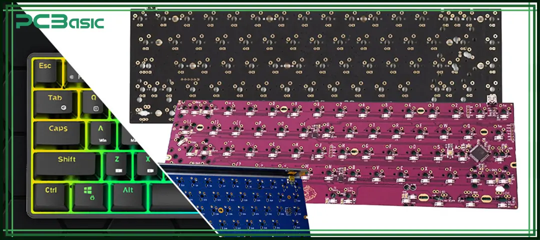
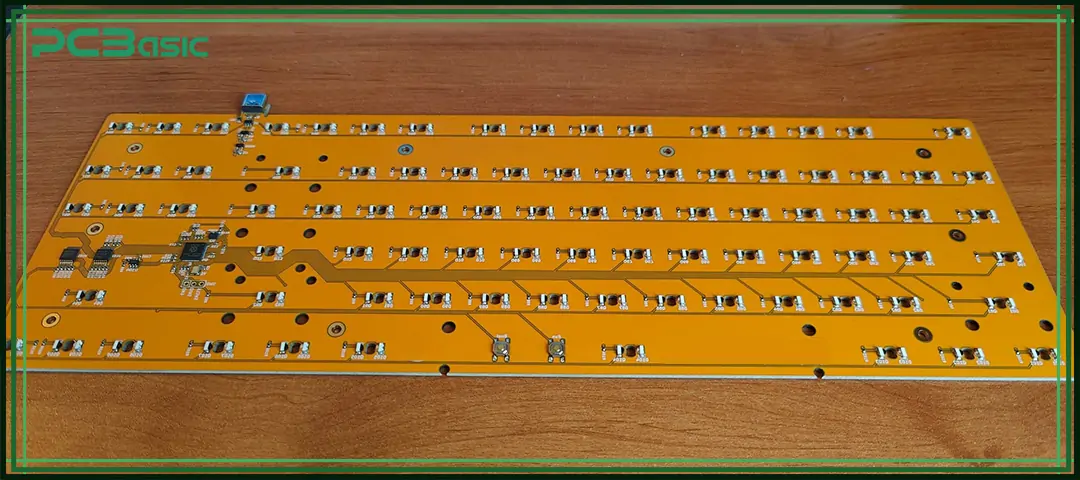
A keyboard PCB is a keyboard circuit board specifically designed for keyboards, which is used to electrically connect keys, diodes and microcontrollers to form a complete and usable input device. Unlike general-purpose electronic circuit boards, the keyboard PCB focuses on optimizing the matrix scanning, key placement accuracy, and the ability to withstand repeated mechanical stress during design.
In simple terms, what is a keyboard PCB? It is the foundation for realizing the basic functions of a keyboard, enabling it to:
• Detect key presses
• Communicate with a computer
• Support firmware and key mapping
• Maintain long-term reliability
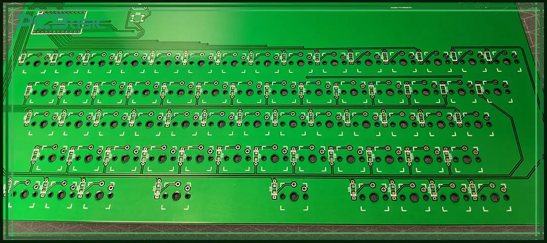
Each mechanical keyboard PCB uses a grid of rows and columns to efficiently register key press. The design of this matrix is one of the most crucial and core parts of keyboard PCB design.
Different keyboards have different requirements for PCBs. Therefore, when conducting keyboard PCB design, it is necessary to select an appropriate solution based on the actual usage. Understanding the common types of keyboard PCBs can help us reduce the cost of trial and error in the design of a keyboard PCB project.
A mechanical keyboard PCB is mainly used for installing mechanical switches, such as Cherry MX and its compatible variants. When designing this type of PCB, the accuracy of the switch hole placement, the strength of the solder pads, and the reliability under long-term use are given priority consideration.
A custom keyboard PCB is a PCB designed separately according to specific requirements. It is commonly seen in non-standard layout keyboards, such as split keyboards, ergonomic keyboards, or keyboards with special function keys.
DIY keyboard PCBs are usually designed and assembled by individuals or small teams on their own. This type of project places more emphasis on the learning process and design freedom, and is often used in experiments, personal use or open-source projects.
Some keyboard PCBs support hot-swap sockets, allowing users to replace the switches without soldering, making maintenance and replacement more convenient. In contrast, soldered PCBs require the switches to be directly soldered onto the board, making the structure more stable.

In keyboard PCB design, whether the early planning is sufficient often determines whether a PCB can be used smoothly or needs to be reworked constantly during the testing stage. Before starting how to design a keyboard PCB, the following points need to be clarified first.
The first step is to determine the size and layout of the keyboard, such as 40%, 60%, 65%, TKL or full size. Once the layout is determined, the switch spacing, stabilizer positions and overall routing structure are basically determined as well.
The keyboard standards used vary by region. The common ones are ANSI and ISO. There are obvious differences in the size and position of the keys between the two, which will directly affect the hole positions and footprint design of the keyboard PCB.
Different switches correspond to different PCB footprints and cannot be mixed arbitrarily. Meanwhile, the type and mounting method of the stabilizers will also occupy PCB space, affecting the pad spacing and routing density.
PCB manufacturers have defined limits on minimum trace width, drill size, and layer count. If these manufacturing conditions are ignored in the early stage of design, the design often needs to be revised later. Considering these limitations in advance can effectively reduce rework and costs in keyboard PCB design.

Time is money in your projects – and PCBasic gets it. PCBasic is a PCB assembly company that delivers fast, flawless results every time. Our comprehensive PCB assembly services include expert engineering support at every step, ensuring top quality in every board. As a leading PCB assembly manufacturer, we provide a one-stop solution that streamlines your supply chain. Partner with our advanced PCB prototype factory for quick turnarounds and superior results you can trust.
This part will be practice-oriented and introduce how to design a keyboard PCB in a repeatable and implementable way.
The schematic diagram is the electrical blueprint of the keyboard PCB; the main contents include:
• Microcontroller selection
• Switch matrix wiring
• Diode placement
• USB power and ESD protection
When designing the schematic diagram of the keyboard PCB, a clear structure is very important. A clean and standardized schematic diagram can significantly reduce the later debugging time and improve the long-term maintainability of the keyboard circuit board.
PCB layout is a crucial stage for keyboard PCB design to move from the blueprint to the physical product. The key factors that need to be focused on include:
• Switch alignment accuracy
• Consistent row and column routing
• Short, clean signal paths
• Proper grounding
For a mechanical keyboard PCB, mechanical tolerances are as important as electrical designs. Unreasonable placement of components may cause switch misalignment or solder joint stress.
Before sending the design for production, the following checks need to be completed:
• Run design rule checks (DRC)
• Verify footprints and polarities
• Review USB routing and power paths
These final checks are crucial for the DIY keyboard PCB project and help ensure that the keyboard PCB works properly during the first prototyping.

A keyboard PCB is incomplete without firmware.
Popular firmware platforms allow you to:
• Define key mappings
• Create layers and macros
• Update layouts without redesigning hardware
Firmware compatibility should be considered early in keyboard PCB design, especially when choosing MCU pins and matrix size.
For anyone learning how to make keyboard hardware, firmware integration is often the final step that turns a keyboard circuit board into a usable product.
Even experienced designers encounter issues in keyboard PCB design. Common mistakes include:
• Incorrect diode orientation
• Poor USB grounding
• Overcrowded routing
• Ignoring mechanical tolerances
• Choosing unsupported MCUs
Avoiding these mistakes significantly improves the success rate of custom keyboard PCB projects and reduces rework costs.
Learning keyboard PCB design essentially means mastering the core ability of keyboard customization. Just figure out what a keyboard PCB is and how keyboard PCB functions, and how to design a keyboard PCB step by step, you can have a clear idea of the layout, functions and stability of the keyboard.
Whether it's making a DIY keyboard PCB, developing a custom keyboard PCB for personal use, or attempting small-scale production, as long as the basic and reliable keyboard PCB design principles are followed, the project is more likely to succeed on the first attempt. If your goal is to design your own keyboard, truly understanding and mastering the keyboard circuit board is the most important step in the entire process.
As long as the early planning is clear, the layout design is reasonable, and it is ensured that the firmware matches the hardware, the keyboard PCB design will no longer be a complex and difficult thing to understand, but a process that has both engineering value and practical achievement.

Assembly Enquiry
Instant Quote
Phone contact

+86-755-27218592
In addition, we've prepared a Help Center. We recommend checking it before reaching out, as your question and its answer may already be clearly explained there.
Wechat Support

In addition, we've prepared a Help Center. We recommend checking it before reaching out, as your question and its answer may already be clearly explained there.
WhatsApp Support

In addition, we've prepared a Help Center. We recommend checking it before reaching out, as your question and its answer may already be clearly explained there.