Global high-mix volume high-speed PCBA manufacturer
9:00 -18:00, Mon. - Fri. (GMT+8)
9:00 -12:00, Sat. (GMT+8)
(Except Chinese public holidays)
Global high-mix volume high-speed PCBA manufacturer
9:00 -18:00, Mon. - Fri. (GMT+8)
9:00 -12:00, Sat. (GMT+8)
(Except Chinese public holidays)
HomePage > Blog > Knowledge Base > Solder Mask Material: A Complete Guide
When discussing the reliability of PCBs, we often associate the problems with copper thickness, surface treatment or solder paste. However, in reality, many soldering defects and long-term failure issues are related to the PCB solder mask material. The solder mask layer is not merely a "green ink layer" on the PCB. The theme of this article is the solder mask material.
Next, this article will systematically introduce the relevant content of solder mask material. This includes its definition, material composition, common types, as well as the properties of solder mask material that engineers are most concerned about in practical applications.
Solder mask material is a protective coating with electrical insulation properties. On a PCB, it is applied to the outer surface, covering and sealing most of the copper lines. Why only cover most of them? This is because the soldering areas (such as pads, component pads, test points, and designated edge connection areas) need to remain exposed in order to meet the assembly requirements.
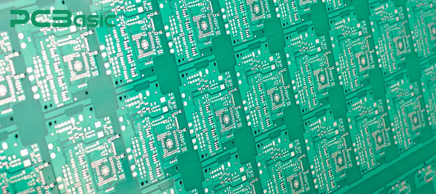
During the PCB manufacturing process, the PCB solder mask material mainly plays the following key roles:
Solder control (assembly yield)
The solder dam can restrict the flow of molten solder, preventing solder bridges between adjacent pads, thereby reducing the risk of short circuits.
Copper foil protection (reliability)
The soldering mask material can isolate the copper surface from air, moisture, residual flux, and other contaminants, reducing the occurrence of oxidation and corrosion.
Electrical insulation (safety and performance)
By increasing the surface insulation resistance, the soldering mask layer can effectively reduce the risk of leakage (especially in high humidity environments).
Mechanical protection (operation and wear)
The cured soldering mask layer can enhance the surface scratch resistance, reducing mechanical damage to the circuitry during production, board separation, transportation, or actual use.
Understanding solder mask material involves not only understanding its impact on assembly defects, but also evaluating its role in ensuring the long-term reliability and electrical safety of the PCB.
Solder mask material is essentially an engineered high-molecular coating system. Typical solder mask materials are usually composed of the following key components:
Base resin: It is the structural core of solder mask materials, commonly being epoxy resin or modified epoxy acrylate system. The type of resin largely determines the hardness of the solder mask material, its adhesion to copper foil and substrate, flexibility, as well as chemical and moisture resistance. Epoxy systems, due to their stable comprehensive performance, are widely adopted in PCB solder mask materials.
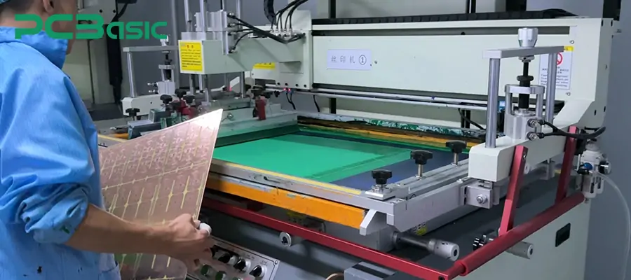
Curing agent / Crosslinking agent: Curing agents are used to promote crosslinking of polymer molecules during thermal curing or UV curing processes, forming a stable network structure. This crosslinked structure endows the solder mask layer with excellent mechanical strength and thermal stability. This is also the key factor that enables PCB solder mask materials to withstand the high temperatures of lead-free reflow soldering and multiple thermal cycles without cracking or peeling.
Photoinitiators: Photoinitiators play a core role in photosensitive solder mask materials (such as LPI solder mask). They react under ultraviolet light exposure, enabling the solder mask layer to undergo precise exposure imaging. Thus, manufacturers can achieve high-resolution window openings and accurate alignment.
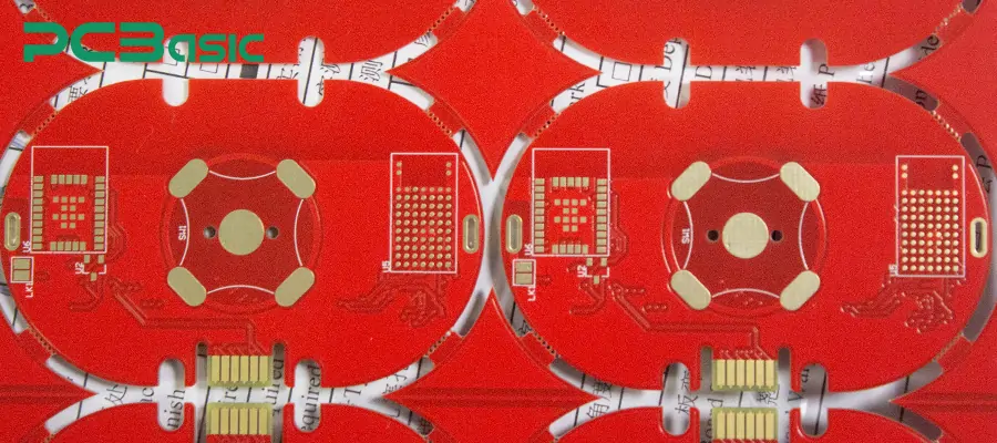
Pigments: Pigments give solder mask materials different colors, such as green, black, blue, red, white or matte black, etc. Color is also part of the functional design of solder mask materials. This is because different colors can affect manual inspection, AOI recognition contrast, and heat absorption during the reflow soldering process.
Fillers and functional additives: These are used to adjust and optimize the properties of solder mask materials, including viscosity control during application, reduction of curing shrinkage, and improvement of flame retardancy, etc. The proper proportioning of these components will directly affect the reliability of PCBs.
After understanding the basic composition of solder mask material, the next step will be to introduce the material forms. In actual PCB manufacturing, solder mask material does not exist in a single form. Depending on the imaging method, coating process and application requirements, solder mask materials come in various types.
|
Solder Mask Type |
Typical Applications |
Key Advantages |
Main Limitations |
|
Epoxy-Based Solder Mask (Screen-Printed) |
Low-density PCB designsLarge pad spacing layoutsCost-sensitive products |
Good mechanical toughnessSimple process flowCompetitive manufacturing cost |
Lower resolution compared to photoimageable solder mask materialDifficult to control uniform thickness in fine-pitch areasNot suitable for modern tight-pitch SMT and BGA designs |
|
Liquid Photoimageable (LPI) Solder Mask |
Fine-pitch SMT and BGA applicationsHigh-density PCBsMost commercial and industrial PCB products |
High pattern resolution for small openingsBetter solder mask registration controlStrong adhesion to copper and laminateStable solder mask material properties under lead-free reflow |
Requires strict process control (surface preparation, exposure, development)Slightly more complex than screen printing |
|
Dry Film Solder Mask |
HDI boardsVery tight geometries and fine featuresApplications requiring highly uniform solder mask thickness |
Excellent thickness consistencyClean and sharp opening edgesStrong solder mask dam control in dense layouts |
Higher material and processing costLamination challenges on uneven surfaces or deep topographyHigh sensitivity to lamination temperature and pressure |
|
UV-Curable Solder Mask |
Applications requiring rapid curingSelective or localized solder mask areasSpecialized or non-standard process flows |
Fast curing speedLower thermal stress compared to long thermal curing processesEfficient for niche applications |
Not always suitable for multiple high-temperature reflow cyclesProperty stability highly dependent on formulation and post-cure conditions |
The following performance indicators of the soldering mask materials are usually regarded as key references in manufacturing and reliability assessment.
1. Adhesion to copper foil and substrate
Adhesion is one of the most fundamental and crucial properties of soldering mask materials. These materials need to firmly adhere to both the copper traces and the PCB substrate surface, requiring sufficient adhesion. If the adhesion is insufficient, it can easily lead to the warping of the pad edges, peeling after reflow soldering, or cracking during thermal cycling. High-quality PCB soldering mask materials should maintain stable adhesion even after multiple lead-free reflow soldering and local repair heating.
2. Heat resistance and lead-free reflow stability
Modern PCB assembly generally adopts lead-free processes, with the reflow soldering peak temperature exceeding 245 °C. Therefore, heat resistance is one of the core indicators of soldering mask materials. Stable PCB soldering mask materials should be able to maintain their original mechanical strength and adhesion performance even after multiple high-temperature cycles.
3. Chemical resistance
During assembly and cleaning processes, soldering mask materials come into contact with flux activators, cleaning agents, and possible residual ionic contaminants. Therefore, good soldering mask materials should also have good chemical resistance to avoid swelling, softening, or surface deterioration of the soldering layer.
4. Electrical insulation performance
Electrical insulation capability is one of the core functions of PCB soldering mask materials. Qualified soldering mask materials should have a high surface insulation resistance (SIR) and maintain stability under high humidity, high bias voltage, etc.
5. Mechanical strength and wear resistance
After complete curing, the soldering mask material needs to form a protective layer with sufficient mechanical strength. Appropriate hardness and scratch resistance can effectively protect the circuit from damage during board separation, mounting, transportation, and assembly. At the same time, the solder mask layer should not be too brittle.
Overall, the performance of the soldering material not only determines the yield rate during the assembly process, but also directly affects the electrical safety, environmental adaptability, and long-term reliability of the PCB.
PCB solder mask material is a functional material in PCB manufacturing that directly affects the stability of production, assembly yield, and long-term reliability. If the solder mask material is improperly selected or the process control is insufficient, it often introduces hidden dangers that are difficult to detect during the production stage but have extremely high costs in actual use.
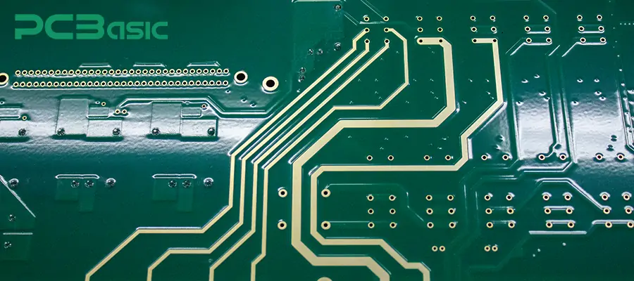
From a manufacturing perspective, the solder mask material plays a crucial role in controlling the soldering process.
1. The appropriate PCB solder mask material can form a stable solder barrier. This ensures effective limitation of solder diffusion during reflow soldering, thereby reducing the risks of bridging and short circuits in fine-pitch SMT and high-density layouts.
2. Solder mask materials with good resolution or adhesion can improve the overall assembly yield when the mounting and solder paste processes are normal.
3. For PCB solder mask materials that need to undergo multiple high-temperature reflow soldering, those with insufficient heat resistance may cause reliability issues. Therefore, it is important to choose solder mask materials with good heat resistance.
At the electrical performance level, PCB solder mask material is also an important component of the PCB insulation system. Stable solder mask material properties help maintain a high surface insulation resistance, reduce the risk of leakage current, and inhibit electrochemical migration phenomena.
In terms of mechanical protection, the cured solder mask layer can effectively protect the copper circuits from scratches and mechanical stress.
Furthermore, the PCB solder mask material also directly affects the consistency and repeatability of mass production. Uniform film thickness, stable curing behavior, and predictable imaging performance help keep the manufacturing process within the controlled range. When the solder mask material performance is stable, PCB manufacturing can achieve higher consistency, higher yield, and higher reliability.
Overall, soldering materials are a crucial factor in PCB manufacturing, significantly impacting product quality, assembly performance, and the entire lifecycle.
In actual production, PCBasic selects the solder mask material based on the wiring density of the circuit board, the assembly method, and the final application scenario of the product. It ensures that the solder mask layer maintains stable and reliable performance throughout the manufacturing process and the product's usage period.
In most consumer electronics, industrial applications, and projects with high reliability requirements, PCBasic mainly uses liquid photosensitive soldering mask (LPI). This PCB soldering material has the characteristics of stable imaging accuracy, controllable film thickness, and strong adhesion to copper foil and substrate. Its overall performance is balanced.
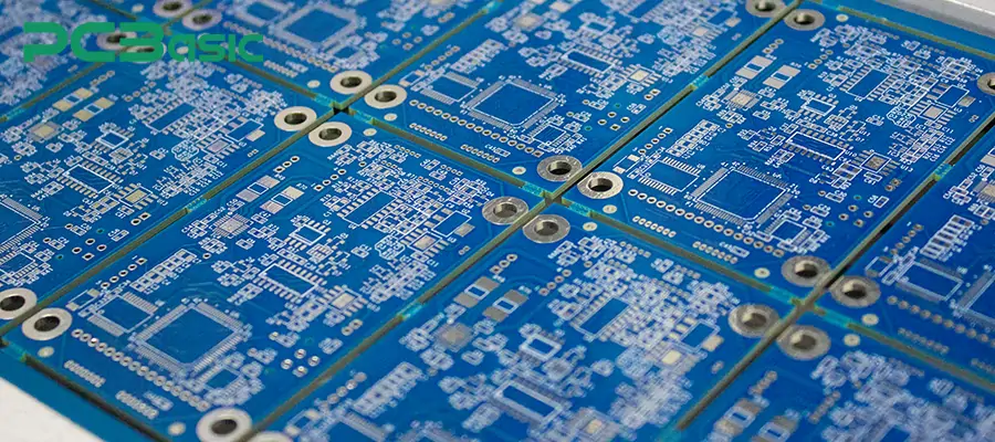
During the evaluation of soldering materials, PCBasic considers heat resistance and process stability as key factors. The selected PCB soldering materials must be able to withstand multiple lead-free reflow soldering processes without issues such as blistering, discoloration, or loss of adhesion. Stable material performance helps to prevent exposed solder pad edges and potential secondary defects that may be introduced during assembly or rework processes.
Electrical insulation performance is also an important criterion for PCBasic when selecting soldering materials. The soldering materials used can maintain a high surface insulation resistance even in high humidity environments and under applied bias voltages. This is particularly crucial for high-density circuits, high-voltage designs, and industrial application environments.
The soldering material used by PCBasic can also support high-resolution imaging and precise alignment, and can maintain a consistent soldering pattern throughout the entire board. This is beneficial for directly improving the assembly yield of fine-pitch and HDI circuit boards.
Based on the default green solder mask, PCBasic also offers a variety of color options such as black, blue, red, white, and matte. The determination of the color is not solely based on appearance; rather, it involves a comprehensive assessment of AOI recognition contrast, manual inspection clarity, and thermal behavior consistency during reflow soldering.
Apart from the material itself, PCBasic also attaches great importance to the control of solder mask process. By strictly managing the coating thickness, exposure energy, development parameters and curing curve, the solder mask material can fully realize its designed performance.
The solder mask material is far more than just an appearance coating. It is a crucial functional structure. It directly affects the assembly yield, electrical insulation performance, mechanical protection capability, and long-term reliability of the PCB. Understanding the solder mask material is not merely about avoiding visible defects on the surface. What is more important is that by learning about the relevant content of the solder mask material, we can reduce potential failure risks, improve consistency in mass production, and ensure that the PCB maintains electrical safety and structural stability in real-world usage environments. It can be said that the reasonable selection of materials and controlled application processes are indispensable key steps for achieving high-quality and reliable PCB manufacturing.
Time is money in your projects – and PCBasic gets it. PCBasic is a PCB assembly company that delivers fast, flawless results every time. Our comprehensive PCB assembly services include expert engineering support at every step, ensuring top quality in every board. As a leading PCB assembly manufacturer, we provide a one-stop solution that streamlines your supply chain. Partner with our advanced PCB prototype factory for quick turnarounds and superior results you can trust.
Assembly Enquiry
Instant Quote
Phone contact

+86-755-27218592
In addition, we've prepared a Help Center. We recommend checking it before reaching out, as your question and its answer may already be clearly explained there.
Wechat Support

In addition, we've prepared a Help Center. We recommend checking it before reaching out, as your question and its answer may already be clearly explained there.
WhatsApp Support

In addition, we've prepared a Help Center. We recommend checking it before reaching out, as your question and its answer may already be clearly explained there.