High-frequency PCB: A Comprehensive Guide
High-frequency PCBs are key elements of state-of-the-art electronics solutions, both for high-speed data transmission and RF/microwave applications. Unlike regular PCBs, high-Frequency PCBs require highly specialized materials, including PTFE, Rogers, as well as the use of ceramic-filled laminates, so you can get the performance you expect. Both the rigid and flexible printed circuit boards have to be designed accordingly to keep the signal integrity and control impedance with as little dielectric constant as possible. Such PCBs are extensively used in 5G networks, radar systems, aerospace, and satellite communication, which operate at frequencies above 1 GHz.

What is a High-Frequency (HF) PCB?
A high-frequency printed circuit board (HF PCB) is a printed circuit board designed to operate at frequencies above 500 MHz, often extending into several GHz ranges. These boards are not typical PCBs; maintaining signal integrity at very high speeds poses significant manufacturing challenges.
High-frequency PCBs find their application in high-speed signal transmissions, including 5G communication, radars, satellite technology, as well as advanced medical equipment.
The high-frequency performance of PCB is greatly affected by the characteristics of its dielectric material, in particular, the dielectric constant (Dk) and dissipation factor (Df). A PCB board with high-frequency laminate would need constant impedance and minimal signal losses to be functional.

Key Characteristics of High-Frequency PCB
· Signal Integrity Requirements
In high-Frequency PCBs, signal integrity quickly becomes one of the most difficult aspects of the design as the frequency gets higher and higher. In short, losses in the signal path from dielectric absorption, radiation, and conductor imperfections may have a significant impact on performance. Routing, grounding, and material selections are aspects that are being considered by designers to minimize these losses.
· Low Dielectric Loss
Low Df (dissipation factor) materials are typically preferred, which allow signals to get to their destination faster and with less loss of strength from signals (from energy being lost), which becomes more of a factor in 5G high-frequency PCB applications.
· Controlled Impedance
Signal timing and quality are a function of controlled impedance. For HF PCBs, trace impedance must align with the system requirements; therefore, reflections, signal degradation, or attenuation will be prevented.
High-Frequency PCB Design Considerations

Designing a high-speed PCB needs more than normal PCB layout ability. Special measures must be taken to achieve GHz operation.
Signal Routing
Routing Methods (Microstrip vs Stripline)
|
Feature
|
Microstrip
|
Stripline
|
|
Trace Position
|
The outer, one side is exposed to air.
|
Inserted between two ground planes.
|
|
Noise Susceptibility
|
Higher, due to air exposure.
|
Lower, due to full shielding.
|
|
Impedance Control
|
Solid, but more environment-driven.
|
Best, highly controlled environment.
|
|
Design Complexity
|
Simpler layout.
|
Complicated, need accurate stacking of layers.
|
Length Matching (Critical for Differential Pairs)
In high-frequency PCB design rules, it is very important to match the lengths of differential pairs. Different length signals result in skew and errors. At the receiver, slight length matches for simultaneous signal arrival.
Via Optimization (Minimizing Count and Stub Effects)
Each via adds to inductance and capacitance, which can distort signals at high frequencies. Improving the signal integrity is accomplished by optimizing via counts and minimizing stub effects.
Crosstalk Mitigation
· Trace Spacing Rules: Sufficient trace separation is one of the simplest methods for minimizing crosstalk in a high-speed PCB. At least three times the width of the trace should be the distance between the traces.
· Ground Shielding Techniques: Adding ground planes and stitching vias around sensitive lines can provide effective shielding, keeping EMI at bay and signal integrity sound.
Impedance Control
· Dielectric Material Selection: Selection of an appropriate dielectric material is the essence for impedance matching. Dk (Dielectric constant) directly contributes to trace impedance, so a material must be carefully selected for the operating frequency.
· Trace Width and Thickness Numbers: Correct trace width and thickness calculations given the selected substrate are necessary to achieve the desired impedance. Impedance calculators, for example, are often used when designing high-frequency PCBs.
High-frequency PCB Materials

Selecting the proper materials to use is critical to a high-frequency PCB that will perform correctly and reliably. There are several different substrate materials. The following are the examples:
· PTFE Rogers, Taconic: PTFE laminates, which include Rogers and Taconic, are used in PCB high-frequency designs because of their extremely low Dk and Df. They have superior electrical properties, but may be too costly and hard to process.
· Ceramic-Filled Hydrocarbons: Hydrocarbon ceramic-filled materials are a cost/performance trade-off. They offer less loss than standard FR-4, while providing better manufacturability than PTFE.
· Altered FR-4 for HF: Some makers provide fast FR-4 that is optimized for higher frequencies. It’s certainly not as high-performing as PTFE or ceramic, but modified FR-4 can be a relatively low-cost option for some specialized high-frequency PCB applications.
Copper Foil Types
HVLP (High Very Low Profile): HVLP copper foil prevents surface roughness reduction and less signal loss, better signal quality at high frequencies.
RTF (Reverse Treated Foil): RTF provides enhanced adhesion without sacrificing roughness for a variety of high-frequency PCB fabrication requirements.
HTE (High Temperature Electrolytic): HTE foils offer high thermal and mechanical strength that can be beneficial when high current and high-frequency performance are required.
Material Selection Criteria

When choosing copper foil for PCB, the copper foil’s roughness, peel strength, and the fit with the base material must be considered for high-frequency laminate. A neat copper finish is optimal to minimize signal attenuation, but not at the expense of performance.
The material selection of high-frequency PCB is a compromise between the electrical performance, thermal performance, process and cost.
· Frequency Range vs. Dk/Df: With increasing operating frequency, dielectrics of low and stable Dk and low Df are needed to reduce signal loss.
· Requirements for Thermal Performance: If the PCB is going to see high temperatures, such as radar or satellite, then there is a need for superior thermal stability materials.
· Trade-Offs between Costs and Performance: There is always a trade-off between performance and cost in any cost-sensitive project. For example, ceramic-filled hydrocarbons can be used in place of PTFE.

PCBasic's High-frequency PCB Manufacturing
At PCBasic, we create high-frequency PCBs and provide world-leading manufacturing services for industries that demand the highest level of precision, reliability, and prompt service for high-speed signals and tightly packed applications.
We focus on custom high-frequency PCBs for clients demanding tailored solutions in the 5G infrastructure, aerospace, automotive radar, and satellite communication markets.
Material Selection
· Uses low-loss dielectric materials, such as Rogers, Taconic, and PTFE-based board material
· Specially selected copper foils with smooth surfaces to lower skin effect loss
Precision Fabrication
· Incredible dielectric thickness control (+/-5% or better)
· The impedance control itself is more accurate (typically ±10% or better)
· Laser drilling of microvias in multilayer layouts
Signal integrity
Signal integrity (SI) is the cleanness and accuracy of an electrical signal traveling through the PCB without distortion, reflection, noise, or loss.
· Small defects or poor designs can cause bad high-frequency PCBs (1, 5, 10 GHz):
· Weakening of the signal (attenuation)
· Reflection (R) (echoes returning)
· Crosstalk (signals crossing each other)
· Timing errors (bits not received properly, etc.)
Signal Integrity Focus
· Trace geometry and spacing.
· Reduced dielectric constant change.
· Controlled roughness of copper surfaces.

Specialized Processes
· Adhesion is enhanced by using plasma for treatment.
· High-end finishes (ENIG, immersion silver, gold plating).
Our high-frequency PCB fabrication factory has rich experience in manufacturing such high-frequency PCBs, from which we can manufacture items meeting customers’ strictest requirements, such as:
· Controlled impedance multilayer HF PCB stack-ups.
· Ultra-low loss laminates: PTFE-based (e.g., Rogers, Taconic) or ceramic-filled.
· Accuracy and etch distance in microstrip and stripline routing.
· Reduction of via stub effects using back-drilling and optimization via design.
Quality assurance is a must, so for that:
· The control system is implemented to maintain the impedance control with a limited tolerance within ±5%.
· 40GHz insertion loss test.
· Thermal cycling (-55°C to +125°C) testing verified.
· Cross-sectioning analysis for plating quality checking.
Specific design services are also provided:
· Stack-up design optimization: Expert guidance on design and optimization of PCB layer stacks to ensure peak electrical performance, ensuing mechanical integrity, and cost effectiveness, especially for complex or high-frequency needs.
· Signal integrity simulations: Sophisticated simulations that predict and reduce disruption due to signal loss, reflection, crosstalk, and EMI, guaranteeing high-speed data reliably transported on the PCB.
· Thermal analysis: Thermal Analysis: Complete thermal modeling and analysis to pinpoint where heat can become an issue, and make design changes to enhance cooling, prolong product life and ensure performance in extreme environments.
· Manufacturability Reviews: Pre-design analysis to make sure the PCB design falls in the set of best manufacturing practices, this will bring to lower production costs, fewer chances of defects, and high fabrication yield.
· Test fixture design: Custom test fixture and system development for fast, accurate testing of PCB assemblies, in line and post-production, to ensure that boards meet all functional and performance criteria.
Applications of HF PCBs

With precise manufacturing capabilities, high-frequency PCBs find their place across a wide range of advanced industries. The market for 5G high-frequency PCB is growing because HF PCB facilitates high-speed data transfer with minimal signal loss, reduced latency, and vast device connectivity, which are the critical thresholds for 5G networks. In communications satellites, the importance of quality, high-frequency signal transmission cannot be overstated. Bespoke high-frequency PCBs that provide the performance characteristics required to survive the harsh environment of space and ensure communications integrity.
High-frequency PCB radar and automotive radar systems are increasingly relying on high-frequency PCB materials to accurately send and receive high-frequency signals at long ranges without distortion.
Diagnostic and treatment devices in medical technology benefit from high-frequency PCBs. These specialized circuit boards are used in MRI machines to generate and process the high-frequency signals necessary for detailed medical imaging. When it comes to surgical applications, RF ablation devices use high-frequency PCBs to provide the optimal energy that allows for less invasive surgical procedures.
The consumer electronics market is adopting higher frequency PCBs to support the requirements for today's wireless communication standards in handheld products. These specialized circuit boards are used in smartphones, tablets, and other mobile devices for 5G antennas, Wi-Fi 6 E/6 modules, and Bluetooth connectivity. Market demand for faster and more responsive data transfer has necessitated these high-frequency PCBs in routers, gaming systems, IoT products, and many other consumer devices.
Conclusion
High-frequency PCBs are a key part of cutting-edge technology, driving advancements from 5G to space exploration. Knowledge of the key components of high-frequency PCB design — signal routing, impedance control, choice of material, and crosstalk isolation — is important to achieve consistent performance in high-speed systems.
At the same time, selecting a high-frequency PCB manufacturer and materials makes a big difference in the board itself meeting the needs of the application. Whether you are designing state-of-the-art radar systems or planning 5G, 6G, or 7G infrastructure, PCB high-frequency design is a critical part of your success.
About PCBasic
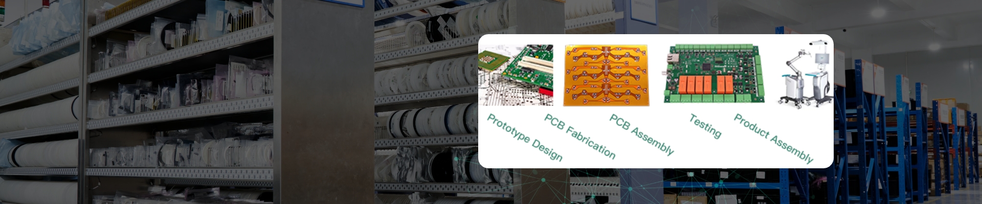
Time is money in your projects – and PCBasic gets it. PCBasic is the pcb assembly company that delivers fast, flawless results every time. Our comprehensive PCB Assembly Services include expert engineering support at every step, ensuring top quality in every board. As a leading PCB Assembly Manufacturer, we provide a one-stop solution that streamlines your supply chain. Partner with our advanced PCB Prototype Factory for quick turnarounds and superior results you can trust.