Global high-mix volume high-speed PCBA manufacturer
9:00 -18:00, Mon. - Fri. (GMT+8)
9:00 -12:00, Sat. (GMT+8)
(Except Chinese public holidays)
Global high-mix volume high-speed PCBA manufacturer
9:00 -18:00, Mon. - Fri. (GMT+8)
9:00 -12:00, Sat. (GMT+8)
(Except Chinese public holidays)
HomePage > Blog > Knowledge Base > What Is Panel Assembly?
Are PCBs assembled one at a time, piece by piece? This is not applicable in the modern era that emphasizes efficiency and precision. To meet the constantly increasing demands, manufacturers have adopted a panel assembly method to optimize the production process and enhance production efficiency.
In simple terms, panel assembly involves combining multiple small boards into one large panel through PCB panelization for production. This way, the entire PCB panel assembly process can be completed all at once on the large panel. This method significantly improves the efficiency and consistency of circuit board production.
Panel assembly is the topic we are going to discuss. Next, we will introduce the definition of panel assembly, its importance, and common PCB panel assembly sheet methods, etc. Without further ado, let's get to the main point!
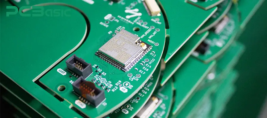
Panel assembly is a widely used production strategy in modern electronic manufacturing. As we mentioned earlier, panel assembly is carried out by assembling multiple circuit boards together into a larger unit for production and assembly. This unit is called "panel".
The process of arranging multiple small boards onto a large board is called "PCB panelization". Once the assembly is completed, the entire PCB panel assembly process will be carried out in a more efficient and equally precise manner. Then, we will separate the circuit boards into finished products through the PCB depanelization method (such as V-Cut, Tab-Routing, milling or laser cutting). Thus, the entire production process is completed.
The use of PCB panel assembly is not only because it is convenient, but also because it is a key method for reducing costs, enhancing reliability, and ensuring smooth production. Its main advantages include:
The greatest advantage of the panel assembly method is the improvement in efficiency. Previously, circuit boards were individually soldered, assembled, and tested one by one. This required a lot more time. However, with the panel assembly method, we can complete the processes for multiple boards at once. Not only does this shorten the machine production cycle and increase equipment utilization; it also allows more finished products to be produced in the same time, speeding up delivery..
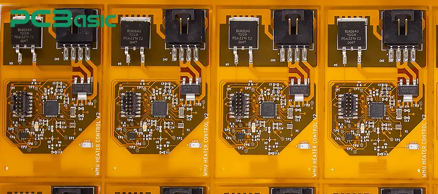
Why does the panel assembly method lead to cost reduction? The reasons are as follows:
① Conducting machine debugging, solder paste printing, and inspection block by block will result in a large amount of repetitive work. This repetitive work also incurs expenses. However, through PCB panelization, the amount of repetitive work can be significantly reduced.
② Using the paneling method, the time for manual handling and intermediate steps will also be reduced, which can greatly save labor costs.
③ Panel assembly can significantly lower the production cost per unit product.
Small-sized, ultra-thin or irregular-shaped PCBs are often relatively fragile. When they are processed and handled individually, they are prone to warping, breaking or damaging the pads. However, if we combine these small boards into a larger panel, the entire panel can achieve better mechanical strength and support. This way, deformation of individual boards can be effectively prevented in subsequent operations. In addition, the large panel is easier to fix and operate than individual small boards, and to some extent, reduces damage and scrapping.
There is not just one single way to assemble PCB panels. We can also use the Pizza Panel (multi-project assembly) method, where different types of PCBs are placed on the same panel. This approach avoids multiple board manufacturing processes, saving manufacturing costs and time. It is indeed a very convenient method. What other panel assembly methods are there?
|
Panelization Type |
Description |
Advantages |
Disadvantages |
Typical Applications |
|
V-Scoring (V-Cut Panelization) |
Shallow V-shaped grooves are cut on the top and bottom along straight lines between adjacent PCBs. Boards remain connected by a thin web and are separated by snapping or using a V-cut machine. |
- Low cost - Fast depanelization - Ideal for high-volume straight-line designs |
- Only supports straight-line panelization, not suitable for curved or irregular boards - Mechanical stress during separation may damage components |
- Smartphones, laptops, and rectangular boards - High-volume consumer electronics |
|
Tab-Routing (with Mouse-Bites) |
PCBs are routed apart with a milling tool, leaving small tabs with perforated “mouse-bite” holes for easy break-off. |
- Supports irregular board shapes - Accurate positioning and flexible layout - Cleaner separation compared to V-score |
- Rough edges after breaking, may require sanding - Some stress still applied during depanelization |
- Automotive electronics - Medical devices - Irregular PCB designs |
|
Solid Panel with Rails (Breakaway Edges) |
Additional border rails are added around the PCB panel to improve strength and allow easier handling on conveyors, printers, and inspection machines. |
- Increases mechanical strength and reduces warpage - Rails provide space for tooling holes, fiducial marks, and barcodes |
- Rails must be removed after assembly, adding an extra depanelization step |
- Very small or thin boards - High-density designs - SMT automated assembly lines |
|
Mixed Panelization (Hybrid) |
Combines both V-scoring and tab-routing methods in a single panel to balance flexibility and cost. |
- High flexibility - Suitable for complex board geometries - Balances cost and quality |
- More complex design - Higher manufacturing requirements |
- Polygonal or irregular boards - High-end PCB projects |
|
Multi-Design Panel (Pizza Panel) |
Different PCB designs are combined into a single panel, similar to pizza slices. |
- Saves tooling cost - Allows multiple small-batch products to share a single production run - Useful for prototypes |
- Increases manufacturing complexity - May affect yield and lead time |
- Multi-project R&D - Small-batch prototyping |
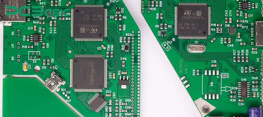
A reasonable PCB panel design not only enhances the assembly and production efficiency of manufacturers, but also helps customers save costs. Moreover, when producing in accordance with strict industry standards and actual manufacturing requirements, a good panel design can also reduce defects and yield losses of PCBs during the board splitting process. When designing, the following aspects should be given particular attention:
1. Panel size and shape. First of all, the size and shape of the designed panel should comply with the requirements of the production line. Regular rectangles are the easiest to assemble; irregular shapes or small panels will require processing edges or Tab-Routing.
2. Pay attention to the layout of components. It is best not to place fragile components such as connectors and crystal oscillators near the board separation lines, as this could cause damage during the board separation process.
3. Remember to add fiducials (alignment marks) and tooling holes to the process area to ensure that the SMT automated equipment can accurately align.
4. The design of the panel should be sturdy enough to withstand handling and reflow soldering, and it should also be convenient for panel separation without causing excessive stress.
5. When designing, the dimensions and requirements of SMT soldering machines, reflow ovens, conveyor belts, etc., should be taken into account. Avoid the situation where batch processing cannot be carried out later. (For more information: PCB Panelization)
IPC-2221 - General PCB Design Standard, covering PCB layout and assembly rules.
IPC-2226 - Design Guidelines for HDI.
IPC-7351 - Definition of Component Pad and Layout Rules.
UL 796 - Printed Circuit Board Standard.
Manufacturer Specifications - Process Capability Description of PCB Manufacturers (provided by the manufacturers).
Before finalizing the PCB panel design, it is essential to take these parameters into consideration.
The PCB panel assembly process we are going to introduce here refers to the workflow of simultaneously producing and assembling multiple printed circuit boards on the same panel.
1. Solder paste printing: The stainless steel mesh is aligned using the global alignment reference points (fiducials) on the panel. Then, the solder paste is printed onto all the pads of the PCBs on the panel at one time.
2. Soldering: The automatic soldering machine will precisely place each component at the corresponding position on the panel according to the settings.
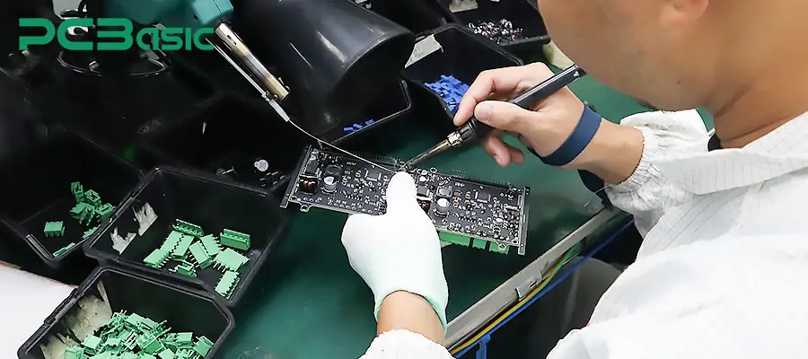
3. Reflow Soldering: The entire panel is placed into the reflow soldering furnace together. During the heating and cooling process, all the solder joints on the PCBs on the panel are formed simultaneously.
4. Inspection: The AOI machine scans each small board on the panel to check the accuracy of component placement and the presence of soldering defects. If there are hidden solder joints such as BGA or QFN, X-ray machines are also used for inspection.
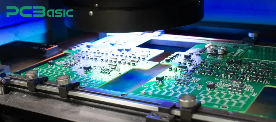
5. Online testing/functional testing: The test fixtures or flying probe testing system can simultaneously test multiple circuit boards, ensuring that only high-quality circuit boards proceed to the next stage.
6. PCB Splitting: After assembly and testing are completed, the large panel is divided into individual small boards.
This is the entire process of panel assembly. Next, we will introduce several common methods for PCB splitting to you.
|
Method |
Description |
Pros |
Cons |
|
V-Scoring |
Shallow V-shaped grooves are cut along panel lines, boards are snapped apart manually or with machines. |
- Low cost - Fast separation |
- Limited to straight-line cuts - Can cause mechanical stress |
|
Tab-Routing |
Boards are connected by small breakaway tabs, removed by breaking, cutting, or specialized depaneling machines. |
- Supports complex board shapes - Flexible panelization |
- May leave rough edges - Stress during breaking |
|
Router Depanelization |
A router bit mills along the panel separation lines. |
- Precise separation - Suitable for irregular shapes |
- Slower process - Generates dust |
|
Laser Depanelization |
High-precision laser cuts boards from the panel without physical contact. |
- Stress-free- Extremely precise - Works for complex designs |
- High equipment cost - Requires fume extraction |
Panel assembly is an indispensable method in the production of large and small batches of circuit boards. It not only saves money and time, but also ensures quality in large-scale production. A reasonable PCB panel design helps to avoid damage during PCB depanelizaion, and at the same time maximizes the efficiency of PCB panel assembly. Whether you are a designer or a producer, understanding the principles and processes of PCB panel assembly can help you make products more reliable and cost-effective.
Time is money in your projects – and PCBasic gets it. PCBasic is a PCB assembly company that delivers fast, flawless results every time. Our comprehensive PCB assembly services include expert engineering support at every step, ensuring top quality in every board. As a leading PCB assembly manufacturer, we provide a one-stop solution that streamlines your supply chain. Partner with our advanced PCB prototype factory for quick turnarounds and superior results you can trust.
 About PCBasic
Assembly Enquiry
Instant Quote
Phone contact

+86-755-27218592
In addition, we've prepared a Help Center. We recommend checking it before reaching out, as your question and its answer may already be clearly explained there.
Wechat Support

In addition, we've prepared a Help Center. We recommend checking it before reaching out, as your question and its answer may already be clearly explained there.
WhatsApp Support

In addition, we've prepared a Help Center. We recommend checking it before reaching out, as your question and its answer may already be clearly explained there.