Global high-mix volume high-speed PCBA manufacturer
9:00 -18:00, Mon. - Fri. (GMT+8)
9:00 -12:00, Sat. (GMT+8)
(Except Chinese public holidays)
Global high-mix volume high-speed PCBA manufacturer
9:00 -18:00, Mon. - Fri. (GMT+8)
9:00 -12:00, Sat. (GMT+8)
(Except Chinese public holidays)
HomePage > Blog > Knowledge Base > What is a PCB Via?
Although the PCB via is one of the smallest structures on the circuit board, it plays the most crucial role: enabling the transmission of electrical signals, power and even heat between different layers. Without vias in PCBs, multilayer circuit boards cannot be realized.
So, what is a via in the PCB? This is a fundamental issue that every PCB designer, engineer and student must master. This article will introduce different types of vias - including through-hole, blind, buried, microvias, etc. Meanwhile, it will analyze the via covering and filling processes that comply with IPC standards, such as tended vias, plugged vias, filled vias, and capped vias. Furthermore, this article will explain the design rules, including the via aspect ratio and the microvia aspect ratio, and how manufacturing methods such as via drilling affect cost and reliability.
After reading this article, you can not only accurately understand the definition of a PCB via, but also learn how to select the appropriate PCB via types in the design, optimize the layout to reduce EMI, consider manufacturability, and use vias correctly in various applications, ensuring the performance and long-term reliability of the circuit board.
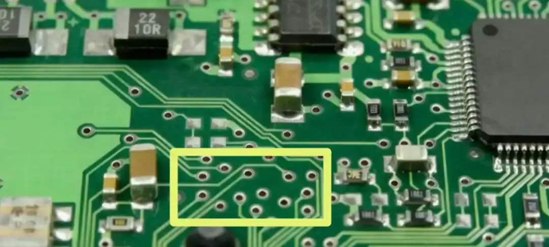
A PCB via is a small hole drilled on a printed circuit board and plated with copper, used to allow electrical signals, power, or heat to pass between two or more layers. In simple terms, a PCB via is a vertical interconnect that can connect traces, planes and components on different layers of the circuit board. Without vias in PCBs, it would be impossible to manufacture today's multilayer circuit boards.
Unlike a plated-through hole (PTH) used for mounting component leads, the PCB via does not insert leads. Its sole function is to serve as a conductive channel, enabling connectivity between layers. This difference is very crucial: PCB vias are only used for vertical signal transmission or power distribution, thus saving surface space for components and routing.
In modern electronics, the significance of vias goes far beyond connectivity. Different via types, such as through-hole, blind, buried and microvias, respectively, meet different requirements for density, performance and cost.
In short, if copper traces are highways of a PCB, then PCB vias are the tunnels that connect different layers of the highways. They can not only ensure the stability of electrical and thermal performance, but also support the miniaturization and high complexity of modern electronic devices.
When we try to understand what a via is in the PCB, it is not only about knowing its definition, but more importantly, understanding its role in the circuit board.
Vias in PCBs allow signals to pass vertically through the circuit board, enabling smooth interconnection between different layers. It is precisely for this reason that designers can achieve multilayer routing in a limited space.
In multilayer PCBs, power planes and the ground planes need to be interconnected, which must rely on different types of vias. Through these vias, voltage can be stably transmitted and shorter return paths can be formed, making power distribution more reliable.
The surface space is extremely valuable. Designers usually use different PCB via types to hide the traces in the inner layers. In this way, more space can be left on the surface of the circuit board for components such as chips, capacitors and inductors.
Via design not only affects connectivity, but is also directly related to signal quality. A reasonably designed via can reduce impedance discontinuities, lower crosstalk and EMI (electromagnetic interference).
High-power chips such as MOSFETs, CPUs or power ICs generate a large amount of heat during operation. Designers will add a large number of thermal vias in the PCB below or near the chip to transfer heat to other layers or larger areas of copper foil in order to dissipate heat more quickly.
In terms of manufacturing technology, the advancement of via drilling techniques has given circuit board design greater flexibility. Mechanical drilling is suitable for conventional through holes, while laser drilling supports smaller and more precise microvias, making high-density interconnects (HDI) possible.
Not all vias are the same. Different PCB via types will be selected according to the design goals - whether it is to save space, improve heat dissipation, or maintain signal integrity. The following introduces the common via types and their roles in PCB design.
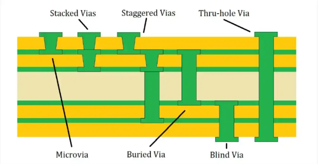
|
Via Type |
Definition |
Advantages |
Disadvantages |
Typical Applications |
|
Through-Hole Via |
Extends from the top to the bottom of the PCB, passing through all layers |
Low cost, simple manufacturing, adds mechanical strength |
Takes up more board space, not always needed on all layers |
Standard PCBs, basic interconnects in multilayer boards |
|
Blind Via |
Connects an outer layer (top or bottom) to one or more inner layers, without going through the whole board |
Saves valuable surface space, ideal for high-density designs |
More complex to manufacture, drilling must stop at a precise depth |
HDI PCBs, under fine-pitch BGAs |
|
Buried Via |
Located completely within internal PCB layers, invisible from the outside |
Frees up outer layers for routing and components |
Higher cost, requires sequential lamination, and longer lead time |
Complex multilayer PCBs, dense routing |
|
Microvia |
Defined by IPC as ≤150 μm diameter, laser-drilled, typically cone-shaped, depth ≤0.25 mm |
Essential for HDI, supports miniaturization, reliable (microvia aspect ratio ~0.75:1) |
More expensive, requires advanced drilling technology |
Smartphones, servers, RF circuits, HDI PCBs |
|
Skip Via |
Connects non-adjacent layers, skipping intermediate ones |
Reduces trace length, improves high-speed signal integrity |
Complex process, less commonly used |
High-speed PCBs, high-frequency applications |
|
Via Type |
Definition |
Advantages |
Disadvantages |
Typical Applications |
|
Thermal Via (thermal vias in PCB) |
Multiple vias placed under or near high-power devices (e.g., MOSFETs, CPUs, power ICs) to transfer heat to inner layers or copper planes |
Improves heat dissipation, lowers inductance when used in parallel |
Consumes board area, requires careful thermal analysis |
Power electronics, CPUs, high-current circuits |
|
Via-in-Pad (VIP) |
PCB via placed directly inside the pad of SMT components, such as BGA or QFN |
Saves space, shortens current paths, reduces inductance, and improves heat flow |
Requires filling, copper capping, and planarization for reliable soldering |
HDI PCBs, fine-pitch BGAs, high-frequency designs |
|
Stacked Vias |
Multiple vias aligned vertically across layers |
Enables compact routing in dense HDI designs |
More expensive, higher risk of reliability issues |
Smartphones, advanced HDI PCBs |
|
Staggered Vias |
Vias are offset layer by layer rather than aligned |
Reduces EMI, lowers manufacturing risk, and is more reliable |
Takes slightly more space compared to stacked vias |
Automotive, aerospace, high-reliability PCBs |
According to the IPC-50M standards, vias can also be classified by covering and filling methods, which directly affect solderability, reliability and cost:
• Tented Vias – via openings are covered with solder mask to prevent solder wicking during assembly.
• Plugged Vias – partially filled with non-conductive epoxy, commonly used under BGAs.
• Filled Vias – completely filled with conductive or non-conductive materials, improving long-term reliability.
• Filled + Capped Vias – vias are filled and then capped with copper plating, essential in via-in-pad (VIP) designs.
• Other subtypes combine tenting, plugging, and covering processes depending on the design needs.
For instance, tented vias can serve as insulation, filled vias can enhance the reliability of BGA, and filled + capped vias are an indispensable step in the VIP process. Each process brings different costs and complexities. Therefore, choosing the appropriate PCB via types is the key to balancing performance and manufacturability.
Time is money in your projects – and PCBasic gets it. PCBasic is a PCB assembly company that delivers fast, flawless results every time. Our comprehensive PCB assembly services include expert engineering support at every step, ensuring top quality in every board. As a leading PCB assembly manufacturer, we provide a one-stop solution that streamlines your supply chain. Partner with our advanced PCB prototype factory for quick turnarounds and superior results you can trust.
|
Parameter |
Description |
|
Pad Size |
Overall via diameter |
|
Drill Size |
Diameter of the drilled hole |
|
Annular Ring |
(Pad – Drill) ÷ 2; larger rings improve reliability but consume more space |
|
Parameter |
Recommended Value / Note |
|
Via Aspect Ratio |
PCB thickness ÷ via drill diameter |
|
Through-Hole Ratio |
≤10:1 |
|
Microvia Ratio |
≤0.75:1 |
|
Note |
Higher aspect ratios are harder to plate reliably and may cause defects |
|
Parameter |
Impact |
|
Capacitance |
Increases with larger pad/anti-pad sizes |
|
Inductance |
Increases with via length |
|
Effect |
Both affect high-frequency signals, causing reflections and delays |
|
Type |
Function |
|
Stitching Vias |
Tie ground planes together, suppress EMI, and improve shielding |
|
Transfer Vias |
Provide return paths when signals cross reference planes |
|
Consideration |
Note |
|
Differential Pair |
Keep the number of vias equal in both traces |
|
Skew |
Unequal via counts create skew, degrading high-speed performance |
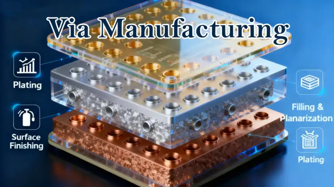
There are mainly two ways of drilling:
• Mechanical Drilling: Mainly used for through-hole vias, suitable for large diameters, with fast processing speed and mature technology, and widely applied in PCB manufacturing.
• Laser Drilling: Commonly used in microvias and blind vias, it can achieve fine drilling with diameters ≤150 μm, meeting the requirements of high-density interconnect (HDI).
Copper deposition is carried out on the drilled through-hole walls to form conductive channels. This step ensures that signals, power or heat can be stably transmitted through the via.
In the via-in-pad process, vias must be fully filled with non-conductive or conductive materials, and then the via is copper-capped and planarized to ensure that the surface is flush with the pad.
Surface finishing of the circuit board is carried out to enhance solderability and prevent oxidation of the via copper. Common finishes include HASL, ENIG, ENEPIG, etc.
• Blind via drilling: Must stop precisely at a specific depth. Even slight deviations can lead to via failure.
• Buried vias: Must be processed and plated before lamination. This requires sequential lamination, which increases cost and production time.
• Microvias: If the microvia aspect ratio is not well controlled, they are prone to interconnect defects (ICD), which can cause open circuits or reduce long-term reliability.
PCB vias are the smallest but most crucial basic units in every modern printed circuit board. Whether it is through-hole vias, blind vias or thermal vias, each via type plays an important role in signal routing, power delivery and thermal management.
By understanding the advantages and disadvantages of via aspect ratio, microvia aspect ratio, via drilling and different PCB via types, designers can strike the best balance among cost, performance and reliability.
Q1: What is the difference between a via and a plated-through hole?
A plated-through hole (PTH) is typically used for mounting components. A PCB via is only used for interlayer electrical connection without component leads.
Q2: Why are microvias important for HDI PCBs?
Microvias in PCB allow fine-pitch BGAs to be routed, reduce crosstalk, improve signal integrity, and support compact HDI designs.
Q3: How do thermal vias improve heat dissipation?
Thermal vias conduct heat away from high-power components to copper planes or heat sinks, lowering temperature and improving reliability.
Q4: What is via tenting, and why is it used?
Tented vias are covered with solder mask to prevent solder wicking during assembly and reduce the risk of short circuits.
Q5: How do vias affect signal integrity at high frequencies?
Improper via design introduces parasitic capacitance and inductance, leading to reflections, delay, and signal degradation. Optimizing via aspect ratio and minimizing via length helps maintain high-speed performance.

Assembly Enquiry
Instant Quote
Phone contact

+86-755-27218592
In addition, we've prepared a Help Center. We recommend checking it before reaching out, as your question and its answer may already be clearly explained there.
Wechat Support

In addition, we've prepared a Help Center. We recommend checking it before reaching out, as your question and its answer may already be clearly explained there.
WhatsApp Support

In addition, we've prepared a Help Center. We recommend checking it before reaching out, as your question and its answer may already be clearly explained there.