Global high-mix volume high-speed PCBA manufacturer
9:00 -18:00, Mon. - Fri. (GMT+8)
9:00 -12:00, Sat. (GMT+8)
(Except Chinese public holidays)
Global high-mix volume high-speed PCBA manufacturer
9:00 -18:00, Mon. - Fri. (GMT+8)
9:00 -12:00, Sat. (GMT+8)
(Except Chinese public holidays)
HomePage > Blog > Knowledge Base > A Comprehensive Guide to Flex PCB Coverlay
With the continuous development of electronic products, flex PCBs are increasingly applied in consumer electronics, automotive electronics, medical equipment and industrial products. Compared with rigid PCBs, flex PCBs often need to withstand bending, folding, vibration and complex operating environments for a long time in practical use, so they have higher requirements for reliability. Under such application conditions, exposed copper traces without a protective layer are very susceptible to mechanical wear, environmental damage or electrical failure. Therefore, the flex PCB coverlay has become an indispensable structural layer.
This article will focus on flex PCB coverlay, providing a detailed introduction to its basic concepts, material structure, working principles, thickness selection guidelines, advantages and limitations, manufacturing processes, as well as precautions in actual design. Whether it is a standard FPC or a more complex rigid-flex PCB, understanding and properly applying the flex PCB coverlay is the key to ensuring the stability and reliability of the product.
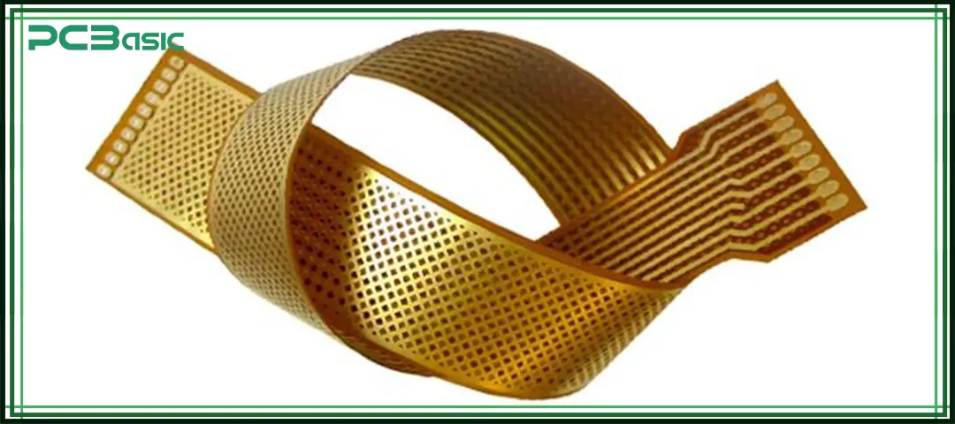
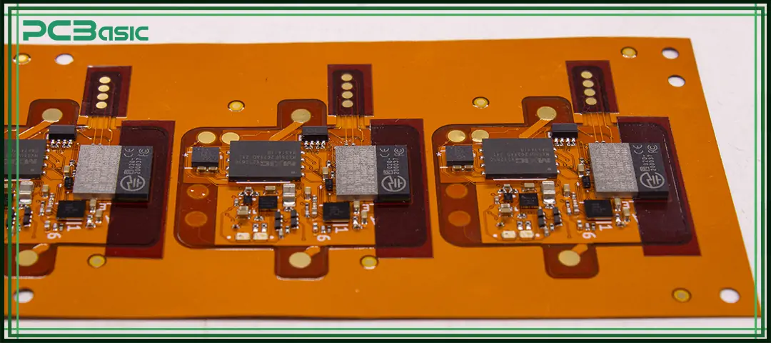
Flex PCB coverlay, also known as coverfilm, is an insulating material used to protect the outer copper traces of flexible circuit boards. Its function is similar to that of the solder mask on a rigid PCB: mainly to prevent the circuit from being directly exposed to the external environment, avoiding moisture damage, mechanical wear, and electrical short circuits.
Unlike the liquid solder mask used in rigid PCBs, the coverlay in flex PCBs is specifically designed for bending applications. It is not prone to cracking when repeatedly bent or moved and can maintain stable performance for a long time. Coverlay is usually provided as a solid film and is bonded to the surface of the flexible circuit by heating and laminating.
In the actual design of flexible PCBs and rigid-flex PCBs, the flex PCB coverlay is generally used in the flexible areas that need to be bent, while the solder mask is still used in the rigid areas. This approach not only ensures the reliability of the flexible area but also benefits the overall manufacturing and assembly.
The structure of the flex PCB coverlay is relatively simple, but it has been highly optimized in terms of flexibility and protective performance. Generally, it mainly consists of the following two parts: polyimide film and adhesive layer:
|
Component |
Polyimide Film |
Adhesive Layer |
|
Material Description |
PI material (e.g., Kapton) |
Acrylic-based or epoxy-based flexible adhesive |
|
Key Characteristics |
High heat resistance, strong mechanical strength, excellent flexibility, and good insulation |
Strong adhesion, good sealing, stress absorption |
|
Role in Flex PCB Coverlay |
Provides insulation, protection, and flexibility; serves as the base layer of flex PCB coverlay |
Bonds the coverlay to copper traces and protects circuitry; critical to the reliability of the coverlay in flex PCB. |
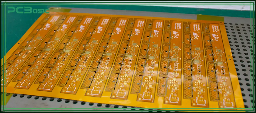
The coverlay in flex PCB is not applied like a solder mask by coating, but is bonded to the circuit surface through a lamination process. The entire process is relatively straightforward and mainly includes the following steps:
Before lamination, the flex PCB coverlay is cut to the required size and shape first, and openings for pads, vias or component positions should be created in advance using laser cutting, drilling or routing.
Align the coverlay accurately with the copper traces on the circuit board to ensure that solder pads are exposed and the rest of the traces are covered and protected.
By heating and applying pressure, the adhesive layer is activated, firmly bonding the flex PCB coverlay to the circuit surface. Vacuum lamination is usually used in production to reduce the risk of air bubbles.
After lamination is completed, the adhesive layer cures, forming a stable bonding structure. Subsequently, the finished boards are inspected to confirm whether the alignment is accurate, the bonding is firm, and whether the insulation performance meets the requirements.
After these steps, the coverlay in the flex PCB will form a sealed and flexible protective layer. When the circuit is bent or moved, it can deform along with the circuit without cracking or delamination, thus ensuring the long-term stable operation of the circuit.
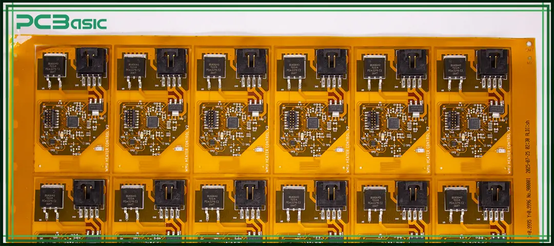
The flex PCB coverlay is important because it plays multiple key roles in flexible circuits:
During the process of circuit bending, folding or assembly, the flex PCB coverlay can effectively protect copper traces and reduce damage caused by friction, vibration and external forces.
The coverlay in flex PCB has good insulation performance and can prevent short circuits between adjacent traces or different copper layers.
The flex PCB coverlay can isolate the circuitry from the external environment, protecting it from moisture, dust, oils and chemical contaminants, thereby enhancing the stability of the circuit in complex environments.
Unlike the solder mask on rigid PCBs, the flex PCB coverlay is less likely to crack when repeatedly bent or moved and can maintain its flexibility for a long time.
By reducing exposure and the risk of physical damage, the coverlay in flex PCB helps to extend the service life of flexible circuits and ensure the long-term stable operation of products.
Time is money in your projects – and PCBasic gets it. PCBasic is a PCB assembly company that delivers fast, flawless results every time. Our comprehensive PCB assembly services include expert engineering support at every step, ensuring top quality in every board. As a leading PCB assembly manufacturer, we provide a one-stop solution that streamlines your supply chain. Partner with our advanced PCB prototype factory for quick turnarounds and superior results you can trust.
When designing a flex PCB coverlay, thickness is a very important factor. The coverlay usually consists of two layers: polyimide film and adhesive layer. The thickness combination of these two layers will directly affect flexibility and protection performance.
• 1 mil PI + 1 mil adhesive (2 mil total): The most common and widely used standard configuration, suitable for most general flexible circuit applications.
• 0.5 mil + 0.5 mil: Ideal for products that require a smaller bending radius and higher flexibility, such as wearable devices.
• 2 mil PI + 1 mil adhesive: Suitable for applications with higher mechanical stress or harsher operating environments, where durability and protection are more important.
• The minimum bending radius the circuit must withstand
• Finished copper thickness (thicker copper typically requires thicker adhesive coverage)
• Insulation and dielectric withstand voltage requirements
• Expected mechanical strength and service life
• Cost limitations
A reasonable selection of the thickness of the flex PCB coverlay can ensure that the circuit is adequately protected while maintaining good flexibility.
• Superior flexibility compared to solder mask
• High mechanical strength and fatigue resistance
• Excellent environmental sealing
• High dielectric strength
• Ideal for dynamic and high-reliability applications
• Higher material and processing costs than the solder mask
• Larger minimum dam size (typically ≥10 mil)
• Not suitable for ultra-fine-pitch components
• More complex manufacturing and alignment process
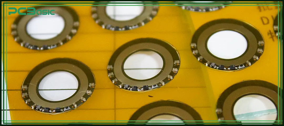
A solder mask is a protective coating applied to the surface of a PCB, mainly used for rigid circuit boards. It is usually liquid photoimageable material (LPI), which is cured on the circuit surface through coating, exposure and development processes.
Although both serve protective functions, flex PCB coverlay and solder mask differ significantly:
|
Feature |
Flex PCB Coverlay |
Solder Mask |
|
Material |
PI film + adhesive |
Liquid photoimageable polymer |
|
Flexibility |
Very high |
Limited |
|
Minimum Dam Size |
~10 mil |
~4 mil |
|
Fine-Pitch Capability |
Limited |
Excellent |
|
Application Area |
Flexible regions |
Rigid regions |
|
Durability in Motion |
Excellent |
Poor |
To ensure the stability and reliability of the flex PCB coverlay, the following points should be noted during the design:
• Clearly specify the coverlay material, thickness, and color in fabrication documents
• Define coverlay openings accurately
• Avoid placing coverlay seams in high-stress bending areas
• Match adhesive thickness to copper weight
• Use coverlay in flex PCB together with solder mask in rigid-flex designs
• Verify bend life and reliability during prototyping
• Communicate with the PCB manufacturer early
The flex PCB coverlay is not merely an additional layer of protection for the circuit, but a key structure for the normal use and long-term reliable operation of flexible circuits. It enables the coverlay in flex PCB to help circuits cope with bending, vibration and complex environments in actual use by providing mechanical protection, electrical insulation and environmental protection.
Only by making correct judgments in material selection, thickness design and manufacturing process, and combining with reasonable design specifications, can the value of flex PCB coverlay be truly brought into play. With the increasingly wide application of flexible PCBs and rigid-flex PCBs, mastering the design and application of coverlays in flex PCBs proficiently will become an important foundation for achieving highly reliable and high-performance electronic products.

Assembly Enquiry
Instant Quote
Phone contact

+86-755-27218592
In addition, we've prepared a Help Center. We recommend checking it before reaching out, as your question and its answer may already be clearly explained there.
Wechat Support

In addition, we've prepared a Help Center. We recommend checking it before reaching out, as your question and its answer may already be clearly explained there.
WhatsApp Support

In addition, we've prepared a Help Center. We recommend checking it before reaching out, as your question and its answer may already be clearly explained there.