Global high-mix volume high-speed PCBA manufacturer
9:00 -18:00, Mon. - Fri. (GMT+8)
9:00 -12:00, Sat. (GMT+8)
(Except Chinese public holidays)
Global high-mix volume high-speed PCBA manufacturer
9:00 -18:00, Mon. - Fri. (GMT+8)
9:00 -12:00, Sat. (GMT+8)
(Except Chinese public holidays)
HomePage > Blog > Knowledge Base > PLCC Package: Guide to Plastic Leaded Chip Carrier Technology
Integrated circuit packaging (IC packaging) directly affects the reliability, size and overall performance of electronic products. As electronic devices continue to evolve towards miniaturization, higher speed and complex functions, packaging technology is also constantly upgrading. Among various packaging forms, the PLCC package has always been a mature solution that takes into account both practicality and cost control.
The plastic leaded chip carrier adopts a compact surface-mount structure and achieves a good balance among mechanical strength, manufacturing convenience, and price. Although in high-performance products, new types of packaging such as ball grid array (BGA) and quad flat package (QFP) have become mainstream choices, the PLCC IC package is still widely used in traditional electronic systems and some professional fields.
This article will systematically introduce PLCC electronics, explaining its structural design, development history, main advantages and disadvantages, mounting methods, and typical application scenarios.
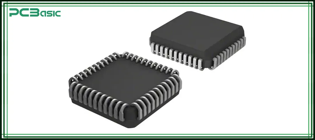
To understand what a PLCC is, it is first necessary to start from its structure and application. PLCC package, the full name of which is plastic leaded chip carrier, is a type of surface-mount integrated circuit package. Its shape is usually square or rectangular, with leads extending from all four sides of the package.
Its main features include:
• J-shaped leads designed for surface mounting
• A plastic-encapsulated body that protects the IC
• Pin counts typically ranging from 20 to 84 or more
• An optional top window for visual inspection of the internal IC
• Can be soldered directly onto a PCB or mounted in a socket
The PLCC package is a solution that has a greater cost advantage than ceramic leadless chip carriers. Compared with leadless chip carriers, PLCC packages have formed pins. This structure can provide better mechanical compliance and is also more convenient for repair and replacement.
The PLCC IC package is commonly found in microcontrollers, ROM devices, programmable logic devices (PLDs), and industrial control systems. Although new packages such as BGA and QFP are gradually becoming popular, PLCC electronics still has practical value in some specific application scenarios.
The plastic leaded chip carrier first appeared in the late 1970s, with the aim of being a low-cost alternative to ceramic packaging. The early PLCC package used a premolded process, which not only had a high manufacturing cost but also a long production cycle. The post-molded PLCC technology that emerged later made the production process simpler, reduced costs, and improved product consistency and reliability.
As the use of PLCC becomes increasingly widespread, the industry has begun to standardize its design. The relevant standards have clearly defined the dimensions, lead pitch, and land patterns of the PLCC package, which enables engineers to directly adopt different package sizes when designing PCBs, and devices from different manufacturers can also be interchanged, thereby simplifying the design work and component sourcing.
It was precisely because of the establishment of these standards that the PLCC IC package gradually became a common packaging format in the 1980s and 1990s, especially being widely adopted in memory devices and embedded systems.
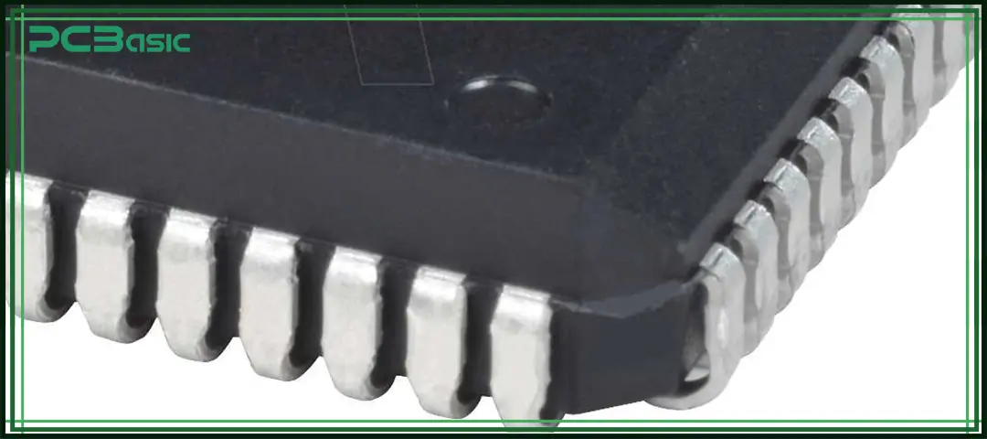
PLCC package usually uses thermosetting plastic as the outer housing material, which can provide excellent insulation and mechanical protection. The leads are generally made of copper or copper alloy and are plated with tin or finished with a lead-free coating, which facilitate soldering onto PCBs.
Compared with ceramic leadless chip carriers, plastic housings are lighter and have a lower cost. Therefore, PLCC packages are more suitable for mass production and use in common electronic products.
Inside the PLCC IC package, the silicon chip is first mounted on the metal leadframe, and then the chip is connected to the leads through bonding wires. Finally, the entire structure will be encapsulated with epoxy resin to prevent the chip from moisture, dust and external mechanical impact.
This design enables the PLCC package to maintain good strength and service life even in a relatively compact size.
The top of each PLCC package has relevant identification markings, which are usually completed by printing or laser engraving. This information includes the manufacturer name, part number, and production date code, facilitating identification, management and quality traceability during the electronic manufacturing process.
Time is money in your projects – and PCBasic gets it. PCBasic is a PCB assembly company that delivers fast, flawless results every time. Our comprehensive PCB assembly services include expert engineering support at every step, ensuring top quality in every board. As a leading PCB assembly manufacturer, we provide a one-stop solution that streamlines your supply chain. Partner with our advanced PCB prototype factory for quick turnarounds and superior results you can trust.
To meet the diverse product design requirements, the PLCC package has evolved into a variety of specifications and forms. Engineers can make their choices based on size, pin count, and the usage environment.
Standard PLCC typically has 20 to 84 pins and is the most commonly used type. It provides a balance between size and functionality, making it suitable for most conventional electronic products.
The miniature plastic leaded chip carrier is more suitable for compact electronic devices with limited space by reducing the package size and pin count.
The thin PLCC IC package reduces the package height without changing the PCB footprint. It is suitable for low-profile products with strict thickness requirements.
The quad-sided PLCC package has leads on all four sides, which can provide more connection points and is suitable for integrated circuits with more pins and more complex structures.
Enhanced PLCC adds a heat sink or heat-spreading structure on the top of the package to improve the heat dissipation. It is suitable for applications with high power or strict thermal control requirements.
Ceramic PLCC uses ceramic material instead of a plastic body, which has better high-temperature resistance and environmental durability. It is often used in high-reliability or harsh working environments.
The PLCC package has several important advantages:
• Cost-effective manufacturing
• Flexible mounting (socket or solder)
• High mechanical stability from J-shaped leads
• Easy inspection and replacement
• Supports off-board programming and testing
Compared with leadless chip carriers, the PLCC design can provide better stress relief capacity and is also more convenient for rework and replacement.
However, the PLCC IC package also has certain limitations:
• Lower thermal dissipation than BGA or QFP
• Limited pin density
• Longer signal paths reduce high-speed performance
• Less suitable for high-power devices
Therefore, although PLCC electronic packaging performs well in terms of reliability, it is not suitable for cutting-edge electronic designs with extremely high requirements for high speed, high frequency or high performance.
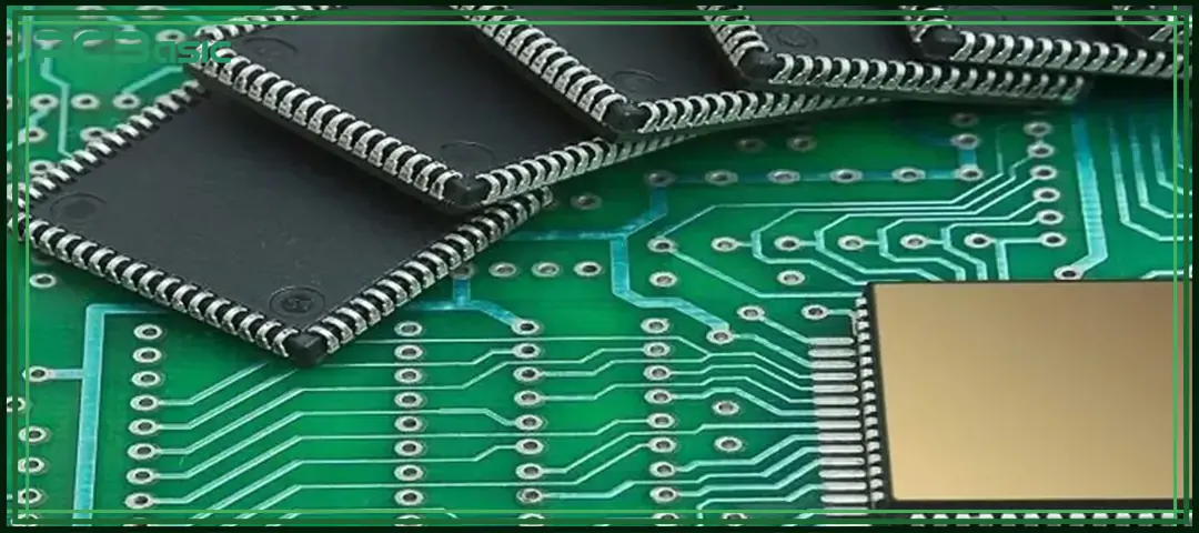
LCC package, the full name of which is leadless chip carrier, is a type of surface-mount integrated circuit package. Unlike PLCC, LCC does not have external leads. Instead, metal pads are set at the bottom edge of the package, and electrical connections are achieved by directly soldering to the PCB through these pads.
Due to its compact structure and stable performance, the LCC package is often used in application scenarios that require high-density mounting and good electrical performance.
|
Feature |
PLCC Package (Plastic Leaded Chip Carrier) |
LCC Package (Leadless Chip Carrier) |
|
Full Name |
Plastic Leaded Chip Carrier |
Leadless Chip Carrier |
|
Lead Structure |
Uses J-shaped leads extending from the package body |
Leadless design with flat metal pads on the bottom |
|
Mounting Method |
Leads are soldered to PCB pads or mounted in sockets |
Bottom pads are directly reflow-soldered onto the PCB |
|
Package Height |
Higher profile |
Lower profile, suitable for thin designs |
|
Mechanical Reliability |
Leads provide stress relief and better mechanical compliance |
Solder joints are more rigid and sensitive to PCB flex and thermal stress |
|
Rework & Replacement |
Easier to remove and replace |
More difficult to rework; often requires heating the entire package |
|
High-Frequency Performance |
Longer signal paths, moderate high-frequency performance |
Shorter signal paths, better for high-frequency and high-speed circuits |
|
Thermal Performance |
Moderate; can be improved with enhanced PLCC (heat sink) versions |
Better thermal performance, especially ceramic LCC |
|
Package Material |
Usually plastic |
Mostly ceramic, with some plastic versions |
|
Cost |
Generally lower |
Usually higher than PLCC |
|
Typical Applications |
Microcontrollers, ROM, PLDs, industrial control systems |
Communication equipment, computer systems, high-reliability electronics |
|
Mounting Flexibility |
Can be soldered or socket-mounted |
Must be directly soldered to PCB |
|
PCB Space Usage |
Slightly larger footprint |
More space-efficient, suitable for high-density layouts |
Through-hole mounting involves inserting the leads of the PLCC package into the holes on the PCB and then soldering them on the opposite side of the circuit board. This method provides strong and stable connections, but it occupies more PCB space and has a relatively higher production cost.
SMT mounting involves directly soldering the PLCC package onto the pads on the PCB surface. This approach is suitable for automated production, which can increase component density and reduce manufacturing costs.
However, it has relatively high requirements for soldering temperature and process; otherwise, thermal stress may affect the reliability of solder joints or devices.
Socket mounting involves inserting the PLCC IC package into the socket, rather than directly soldering it onto the PCB. This method is more convenient for replacement and maintenance, and can also avoid damage to the chip caused by high soldering temperatures. However, it will increase costs and may have a certain impact on signal performance.
Despite the emergence of newer package technologies, PLCC electronics still hold an important position in multiple industries. The main applications include:
• Consumer Electronics: televisions, cameras, laptops
• Automotive Electronics: engine control units, lighting systems
• Medical Devices: diagnostic and monitoring equipment
• Aerospace and Defense: avionics and communication systems
• Industrial Equipment: PLCs and automation controllers
• Memory and ROM Devices: firmware storage
The reason why these industries still widely adopt plastic leaded chip carriers is precisely that it strikes a good balance between durability and cost.
The PLCC package is of great significance in the development process of integrated circuit packaging. It combines the J-shaped leads with the plastic body, enabling the device to achieve more connections in a smaller volume, while enhancing structural stability and reducing the cost of large-scale production.
Although new packages such as BGA and QFP are more widely used in modern electronic products nowadays, PLCC IC packages are still used in many traditional systems and specific application scenarios. Understanding what PLCC is, as well as its structural features, advantages and disadvantages, can help engineers choose a more suitable chip carrier package in the design.
What is a PLCC package?
A PLCC package (Plastic Leaded Chip Carrier) is a surface-mount IC package with J-shaped leads on all sides. It offers a compact footprint, mechanical reliability, and ease of soldering.
Difference between PLCC and LCC
The PLCC has external leads, while the LCC package (leadless chip carrier) uses bottom contact pads. PLCC is easier to rework; LCC offers better thermal and high-frequency performance.
Suitability for high-frequency use
The PLCC IC package is suitable for low- and mid-frequency designs. For RF or very high-speed applications, leadless chip carriers or BGA packages are usually preferred.
Thermal management considerations
Thermal management for PLCC electronics includes heat sinks, PCB thermal vias, airflow design, and careful placement of high-power components.
Typical pin counts and applications
Typical PLCC package pin counts range from 20 to 84. Applications include microcontrollers, ROM devices, industrial controllers, and automotive electronics.
Assembly Enquiry
Instant Quote
Phone contact

+86-755-27218592
In addition, we've prepared a Help Center. We recommend checking it before reaching out, as your question and its answer may already be clearly explained there.
Wechat Support

In addition, we've prepared a Help Center. We recommend checking it before reaching out, as your question and its answer may already be clearly explained there.
WhatsApp Support

In addition, we've prepared a Help Center. We recommend checking it before reaching out, as your question and its answer may already be clearly explained there.