Global high-mix volume high-speed PCBA manufacturer
9:00 -18:00, Mon. - Fri. (GMT+8)
9:00 -12:00, Sat. (GMT+8)
(Except Chinese public holidays)
Global high-mix volume high-speed PCBA manufacturer
9:00 -18:00, Mon. - Fri. (GMT+8)
9:00 -12:00, Sat. (GMT+8)
(Except Chinese public holidays)
HomePage > Blog > Knowledge Base > PCB Schematic: Complete Guide to Circuit Board Design and Layout
In the process of PCB design, a well-crafted PCB schematic is the core foundation for achieving a reliable, stable and fully functional printed circuit board design. A PCB schematic is like a blueprint of the circuit, clearly showing the connection relationship between each component. Whether you are developing a complex microcontroller control system or designing a simple LED driver circuit, learning to draw and understand PCB schematics is an indispensable ability.
This will introduce in detail the concept of PCB schematic and its important role in PCB circuit design, and teach you how to read circuit schematic correctly. Meanwhile, we will also introduce some commonly used tools to help you draw the schematic layout more efficiently and smoothly complete the transition from the schematic to the PCB layout design. By mastering these contents, you can make your PCB design more standardized, clear and easy to manufacture.
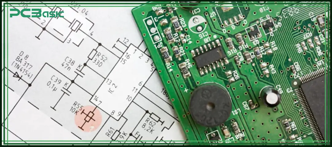
A PCB schematic is a graphical way to represent electronic circuits. It does not directly display the actual positions of components on the circuit board, but expresses the electrical connection relationships among resistors, capacitors, diodes, IC chips, connectors and other components through various standard symbols. Compared with physical layout, schematic diagrams pay more attention to the logical structure and working principle of circuits, which are the first step in PCB circuit design. Typically, a complete PCB circuit diagram records the flow direction of all signals, power connections, and the interaction relationships of key functional modules through schematic capture.
In simple terms, PCB layout design is to actually place these components on the circuit board layout and consider practical issues such as size, heat dissipation, wiring and soldering. A PCB schematic diagram is more like a blueprint of an electrical system, telling us how each component should be connected, how signals should be transmitted, and how circuits should function. Only by first making the schematic diagram and then conducting the PCB layout design can we ensure that the entire circuit board is both logically correct and convenient to manufacture.
A complete and efficient PCB schematic contains the following key elements:
|
Key Element |
Description |
|
Electronic Symbols |
Represent each component in the circuit, such as resistors, capacitors, diodes, and ICs. |
|
Nets or Wires |
Lines showing the electrical connections and indicating signal flow. |
|
Labels and Net Names |
Make the PCB circuit diagram easier to read and allow for clear signal tracing. |
|
Power and Ground Symbols |
Help manage power and ground distribution clearly in the PCB diagram. |
|
Component Designators |
Examples include R1, C2; these identify schematic symbols and link them to physical components on the circuit board layout. |
These elements ensure that the PCB schematic is not only logically correct but also understandable by software and engineers for subsequent PCB layout design.
In the entire PCB board design process, the PCB schematic is the core foundation that determines the success or failure of the design. It is not only the logical blueprint of the circuit, but also directly affects the subsequent routing, debugging and production. Its importance is mainly reflected in the following aspects:
A well-structured schematic layout can fully display the connection relationships and functional logic of each component, thus enabling potential errors to be identified during the design stage and reducing the risk of subsequent functional failures or short circuits.
When there are problems with the circuit board, the circuit board diagram can help engineers quickly locate faulty components or wiring errors, avoiding blind troubleshooting, and significantly improve debugging efficiency.
The PCB schematic is an important technical document in the design process. It not only provides clear references for the engineering team but also helps manufacturers understand circuit logic, ensuring that there will be no misunderstandings during the production process.
Through standardized PCB schematic diagrams, multiple designers can easily understand the overall circuit logic and signal flow, facilitating team collaboration, design review, and modification and optimization.
Modern electronic design tools rely on schematic capture to automatically generate files such as netlist and bill of materials (BOM), and provide precise data support for subsequent PCB layout design.
If a clear and complete PCB schematic diagram is lacking, the entire printed circuit board design process may fall into chaos, and serious design defects are prone to occur, resulting in prolonged debugging and production cycles.
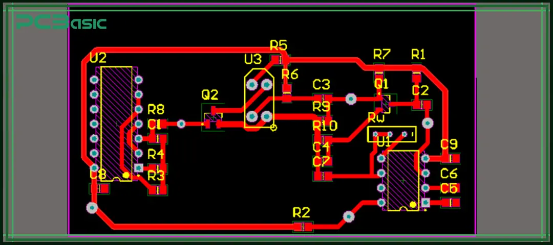
When doing PCB board design, first of all, we need to draw a clear and complete PCB schematic. The schematic diagram needs to ensure the correctness of the electrical logic, as it determines whether the subsequent wiring, debugging and production will go smoothly. Next, let's take a look at the entire PCB schematic design process.
Before starting to draw the PCB schematic diagram, we need to be clear about all the design requirements, including voltage level, signal type (digital or analog), power rating, operating frequency, as well as the limitations of components in terms of size, heat dissipation and packaging. Only by clarifying these requirements can the subsequent PCB circuit design be reasonable and reliable.
Before formally drawing the PCB schematic diagram, we can first draw a simple circuit board diagram or functional block diagram, dividing the circuit into several main modules, such as the power supply section, signal processing section, communication interface or sensor input, etc. In this way, we can have a clear understanding of the circuit structure and discover signal conflicts or design issues in advance.
Let's start drawing the schematic diagram with a professional schematic capture tool. We can place all the components on the drawing with standard symbols, and then connect them according to electrical logic using virtual wires (Nets). This step is like drawing a clear and detailed blueprint for the circuit.
After the schematic diagram is completed, we will add the parameters and designators of the components on the PCB circuit diagram, such as resistance values, capacitance values, chip models, and component numbers like R1, C5, and U2. Clear markings make it more convenient for us to check by ourselves and also facilitate manufacturers to compare materials and determine the soldering position.
Before submitting the schematic diagram, we will check it once using the built-in Electrical Rule Check (ERC) function of the software. It can help us discover unconnected networks, duplicate network names or incorrect connections, avoiding irreparable problems in the subsequent PCB layout design stage.
After confirming that there are no issues with the schematic diagram, we export the Netlist. The netlist serves as a bridge between the PCB schematic diagram and the PCB layout design, recording all electrical connections. After we import the netlist into the board layout software, we can accurately map the logical connections onto the circuit board, achieving a complete transition from circuit design to physical implementation.
Time is money in your projects – and PCBasic gets it. PCBasic is a PCB assembly company that delivers fast, flawless results every time. Our comprehensive PCB assembly services include expert engineering support at every step, ensuring top quality in every board. As a leading PCB assembly manufacturer, we provide a one-stop solution that streamlines your supply chain. Partner with our advanced PCB prototype factory for quick turnarounds and superior results you can trust.
Reading the PCB schematic is an essential basic skill for those engaged in PCB board design or electronic troubleshooting.
A PCB schematic diagram is essentially a visual map that shows the connection methods of each electronic component in a circuit. First of all, we need to identify the power supply and the ground wire, because the voltage rail and the ground symbol show the flow path of electrical energy throughout the circuit board diagram. After figuring out the power line, we can trace the signal path from input to output, especially paying attention to the connections around the microcontroller, operational amplifier and sensor in the PCB circuit diagram.
When reading the schematic diagram, we need to look for modules representing different functions, such as filters, amplifiers, regulators or digital logic gates. Identifying these modules helps us quickly understand the working principle of the entire PCB circuit design. In a schematic layout, each component has a specific function, such as resistors for controlling current, capacitors for filtering or energy storage, etc., while integrated circuits achieve more complex functions.
Meanwhile, reference designators (such as R1, C2, U3) are very crucial because they correspond to the components in the schematic diagram to their actual positions on the circuit board layout, enabling you to conveniently switch between the drawing and the physical PCB during assembly or troubleshooting.
Mastering the reading method of PCB schematics can not only improve the ability of circuit debugging, but also enhance your skills in PCB designing, schematic capture and overall PCB layout design.
Many professional and hobbyist electronic design tools provide a complete PCB design environment, covering the entire process from schematic capture to PCB layout design. Here are some common tools and software for PCB schematic and layout. Let’s have a look:
|
Software |
Features |
|
Altium Designer |
High-end tool with advanced schematic layout and real-time DRC |
|
KiCad |
Open-source, supports full PCB schematic and layout design |
|
Eagle |
Popular among makers and startups, an intuitive PCB diagram editor |
|
OrCAD |
Enterprise-level solution for PCB board design and simulation |
|
EasyEDA |
Browser-based tool for quick PCB schematics and prototyping |
These platforms allow designers to move from circuit board schematic diagrams to final PCB layout designs with minimal friction.
Symbols are the visual language of any PCB schematic. Common circuit board schematic diagram symbols include:
Resistor (zigzag or rectangle) – Limits current


Capacitor (parallel lines) – Stores energy

Inductor (coil) – Stores energy in a magnetic field

Diode (arrow with line) – Allows current in one direction

Transistor – Amplifies or switches signals

Ground – Reference voltage level

Power supply – Voltage source

ICs – Custom symbols representing logic devices or microcontrollers
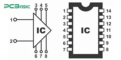
The PCB schematic diagram is the foundation of every successful printed circuit board design. It completely records the logic, structure and intention of the design before the circuit becomes a physical object. Mastering the skill of schematic capture, being familiar with PCB diagram symbols, and making good use of modern design tools can enable engineers to design robust, reliable and easy-to-produce products.
From concept to PCB layout design, the entire process begins with a carefully drawn circuit board schematic diagram. Whether you are just getting started with PCB designing or are improving your skills, you should always prioritize the clarity, consistency and best design standards of the schematic diagram. Your next breakthrough design might start with a well-drawn PCB schematic.
Of course, if you have requirements for PCB design, manufacturing or PCB assembly, you can contact PCBasic, a one-stop PCB solution provider.

Assembly Enquiry
Instant Quote
Phone contact

+86-755-27218592
In addition, we've prepared a Help Center. We recommend checking it before reaching out, as your question and its answer may already be clearly explained there.
Wechat Support

In addition, we've prepared a Help Center. We recommend checking it before reaching out, as your question and its answer may already be clearly explained there.
WhatsApp Support

In addition, we've prepared a Help Center. We recommend checking it before reaching out, as your question and its answer may already be clearly explained there.