Global high-mix volume high-speed PCBA manufacturer
9:00 -18:00, Mon. - Fri. (GMT+8)
9:00 -12:00, Sat. (GMT+8)
(Except Chinese public holidays)
Global high-mix volume high-speed PCBA manufacturer
9:00 -18:00, Mon. - Fri. (GMT+8)
9:00 -12:00, Sat. (GMT+8)
(Except Chinese public holidays)
HomePage > Blog > Knowledge Base > FPGA and ASIC: A Comprehensive Guide
FPGA (full form: Field Programmable Gate Array) and ASIC (full form: Application Specific Integrated Circuit) are two indispensable core technologies in the field of digital hardware development for modern electronic products. The essential differences between them in design methods, flexibility and application scenarios respectively drive technological innovation and industrial upgrading.
With the rapid development of emerging fields such as artificial intelligence and the Internet of Things, discussions about the differences between FPGAs and ASICs have become increasingly prominent. A thorough understanding of the differences between these two technologies can be said to be one of the keys to achieving efficient development, cost control, accelerating product launch and ensuring project scalability. Next, we will systematically sort out the characteristics and comparisons of FPGA and ASIC in this article to assist in better scientific selection and decision-making. OK, let's get to today's topic - FPGA and ASIC.
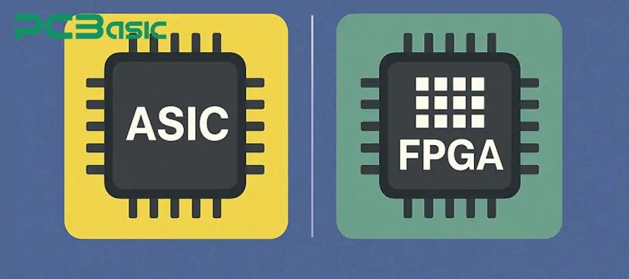
FPGA, also known as "reprogrammable hardware", is a special type of highly flexible integrated circuit (IC). Unlike ordinary chips, the most distinctive feature of FPGA lies in its "programmability". That is to say, the internal structure and functions of a chip are not permanently fixed at the time of leaving the factory. Instead, it allows users to make multiple configurations and programs at the product usage site based on their specific needs.
Inside an FPGA chip, there is a vast array structure composed of tens of thousands of logic units, lookup tables, flip-flops and configurable connections. Users can perform FPGA programming on FPGAs by writing hardware description languages (such as VHDL or Verilog), thereby freely defining the required hardware circuit functions. Whenever the application requirements change, users can rewrite and download the configuration. With this unique reconfigurability, FPGA is widely used in numerous technical fields such as digital logic design, data processing, signal control, and communication systems, and it is an important hardware foundation in modern electronic engineering.
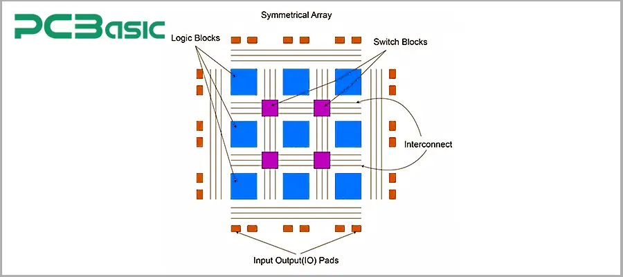
The architecture of FPGA is centered on "programmability" and mainly consists of the following parts:
1. Programmable Logic Blocks
The large number of programmable logic units inside the FPGA chip can implement various basic logical operations (such as AND, OR, NOT, XOR, etc.). They are the basic modules of FPGA design. Users can build complex digital circuit functions by configuring these logic units.
2. Programmable Interconnects
The logic units of an FPGA are connected to each other through a programmable interconnection network. Users can freely define the connection methods between logic units according to their actual needs, allowing signals to flow along the set paths.
3. Input/Output ports (I/O Blocks)
The rich input and output ports enable the FPGA to communicate with external devices, sensors or other chips. The functions and electrical characteristics of each I/O port can also be flexibly configured through programming.
In addition to the above parts, many modern FPGAs also integrate storage units (such as RAM) and dedicated hardware resources (such as DSP modules). The data processing capacity can be further enhanced.
The FPGA programming model refers to the entire process by which users implement the required hardware functions onto the FPGA chip. This process mainly includes:
Hardware Description Language (HDL) development
Users need to write the desired circuit logic and timing in code using a hardware description language (HDL), such as VHDL or Verilog. These codes are equivalent to the detailed "instruction manual" of the chip, telling the FPGA how to work. This step is the most crucial one in FPGA programming.
Synthesis and Implementation
At this step, the development tool will convert the HDL code into a hardware structure that can be implemented on an FPGA chip. This structure includes the allocation of logical units, the configuration of connections, etc.
Download and Configuration
After all the circuit structures have been arranged, the development tool will generate a dedicated "configuration file" (called a bitstream file). Then, the FPGA can implement the corresponding hardware functions based on this file.
Repeated Programming and Upgrading
If the design requirements change, it is only necessary to modify the HDL code, re-synthesize and download it. The FPGA can be "completely renewed" without the need to replace the hardware itself.
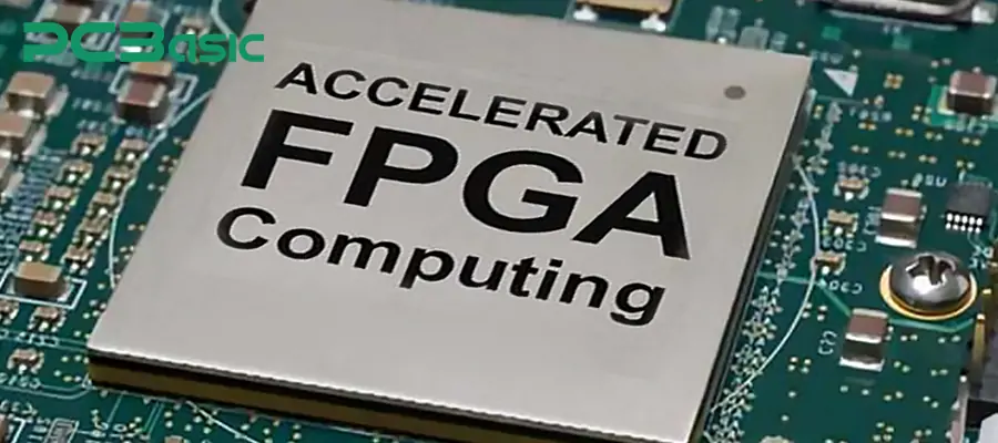
Compared with other hardware solutions, FPGA has multiple advantages.
1. One of the greatest advantages of FPGA is its high reconfigurability. High reconfigurability means that users can still modify or upgrade the hardware functions at any time after the product is deployed to meet new demands or fix bugs without replacing the hardware.
2. The time to market for FPGA is short. Its programmable feature supports rapid design changes and can significantly shorten the development cycle. This is highly suitable for rapid prototyping development and product iteration.
3. FPGA development boards can be flexibly compatible with multiple protocols. It can be customized as needed and supports multiple communication protocols and industry standards.
4. Compared with custom ASICs, FPGAs do not require high mask and manufacturing costs. This makes it particularly suitable for small-batch and medium-batch production.
Although FPGA has many advantages, it also has some limitations.
1. Relatively low performance. Although FPGAs offer extremely high flexibility, they are generally low in terms of speed and energy efficiency. This disadvantage is even more pronounced in high-performance and high-volume applications.
2. The unit price is relatively high in mass production; the individual cost of an FPGA is usually higher than that of an ASIC. This is not conducive to the cost control of ultra-large-scale commercial products.
3. Relatively large in size. FPGA solutions often occupy more board-level space, which is a disadvantage in designs with strict size requirements.
In conclusion, FPGA has many advantages, but it also has disadvantages. It is a hardware solution that combines flexibility and practicality, but when it comes to high performance and large-scale manufacturing, its cost and efficiency need to be balanced.
FPGA is flexible and has powerful parallel processing capabilities, and is widely applied. Its applications include:
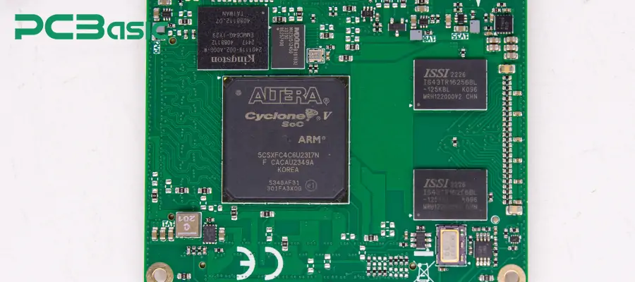
Digital circuit prototype design
Generally, FPGA is the preferred choice for digital circuit prototyping. Because of its reprogrammable feature, functional modification and verification are very convenient. Engineers can quickly implement and test new digital designs, verify system logic, and conduct rapid iterations before moving on to ASIC production.
Hardware acceleration for AI and machine learning
FPGA has parallel data processing capabilities and high-speed logic, which can efficiently handle neural network inference, deep learning computing and edge AI acceleration. This is highly suitable for smart devices and data centers.
Digital Signal Processing (DSP)
The real-time performance and low latency characteristics of FPGA are highly suitable for implementing complex DSP algorithms. DSP applications based on FPGA include audio and video processing, radar signal analysis, medical imaging and wireless communication, etc.
Aerospace and automotive electronics
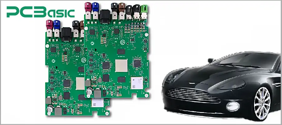
FPGA is also widely used in aerospace and automotive electronic systems due to its high reliability, customizability and ability to meet strict safety standards. Common applications include flight control systems, navigation, in-vehicle infotainment, ADAS, and in-vehicle networks, etc.
In addition to the above-mentioned fields, FPGAs are also widely used in communication and telecommunications infrastructure, storage and data centers. In conclusion, FPGA, with its programmability, high concurrency and flexibility, can be used in almost any situation that requires digital signal processing, custom hardware acceleration or multi-protocol adaptation.
An ASIC is an integrated circuit chip that is custom-designed and manufactured specifically for a particular application or function. Unlike general-purpose chips, ASICs have undergone extreme optimization in structure and performance for a specific niche field or product. It can achieve higher efficiency, lower power consumption and smaller size.
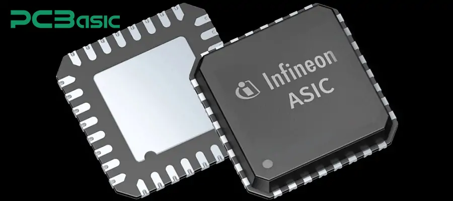
The development process of ASIC is more complex compared to programmable devices such as FPGA and mainly includes the following stages:
1. Requirements analysis and system architecture design
The chip design team needs to conduct a detailed analysis of the required functions, performance goals and interface standards based on application requirements, and formulate the overall chip architecture.
2. Logical design and functional simulation
Then, use hardware description languages (HDL) such as Verilog or VHDL to complete the logic design of the circuit. And verify the correctness of the functions and performance indicators through simulation software.
3. Circuit synthesis and layout design
At this step, engineers will integrate the HDL code into a gate-level netlist and then carry out Layout Design, including the layout and routing of logic units, connections, clock trees, etc.
4. Physical verification and DRC inspection
Then, physical verification is carried out on the completed chip layout. To ensure that all design rules and process specifications (such as DRC, LVS, ERC) fully comply.
5. Tape-out and manufacturing
After that, the design layout is sent to the tape-out production. This step is the main part of the upfront non-repetitive Engineering cost (NRE, non-Recurring Engineering).
6. Testing and Packaging
After the chip manufacturing is completed, the technical team will conduct strict functional tests and performance evaluations on the chip. Then, encapsulation and final system verification are carried out.
7. Mass production and post-maintenance
After verification is passed, it can enter the large-scale mass production stage.
Note: Once the hardware functions of an ASIC are taped out, they cannot be changed. If any changes are needed later, a redesign and tape-out process will be required.
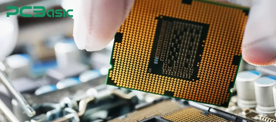
ASIC chips have many unique advantages:
1. ASIC chips are specifically optimized for target applications, featuring faster operating speeds and lower energy consumption. They are the top choice for those pursuing ultimate performance and efficiency.
2. Custom-designed ASICs can integrate more functional modules onto a single chip and achieve a smaller package size. This makes it highly suitable for thin and light devices and highly integrated scenarios.
3. The single-chip cost of ASICs is extremely low, making them highly suitable for commercial products with huge shipment volumes.
4. Customized ASICs will undergo strict testing and optimization. They are highly suitable for critical scenarios such as industry, automobiles, and medical care, where there are extremely high requirements for long-term stability and high reliability.
Of course, ASIC also has its limitations.
1. The design, simulation, tape-out and testing of ASICs require a large amount of engineering investment and financial support. The NRE (Non-Repetitive Engineering Cost) is extremely high, meaning the initial threshold is high.
2. Once the ASIC chip is taped out, its hardware functions are fixed. It cannot be modified as flexibly as FPGA in the later stage. If the functional requirements change, the only option is to redesign and tape-out simultaneously, which will increase the cost and cycle again.
3. The entire ASIC design and manufacturing process is complex and takes a long time. From requirement analysis to final mass production, it usually takes several months to a year or even longer, which is not suitable for projects with frequently changing requirements.
ASIC chips have both advantages and disadvantages and are widely used. Its main applications include:
1. Smartphones and tablets, such as main chips for mobile phones, image processors, baseband chips, dedicated AI accelerators, etc.
2. Data centers and cloud servers, dedicated processors for efficient processing of big data, artificial intelligence computing, cloud acceleration and others.
3. Smart home and Internet of Things (IoT) devices include dedicated control chips for smart speakers, security cameras, smart door locks and other devices.
4. Specialized chips for consumer electronics and wearable devices, such as smartwatches, health monitoring devices, Bluetooth headphones, etc.
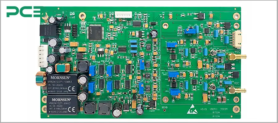
5. High-performance network and communication equipment, such as routers, switches, base stations and other network-specific acceleration chips and communication controllers.
ASIC is a customized dedicated chip solution. It has the advantages of achieving ultimate performance optimization, size integration and large-scale cost. However, it also needs to bear high upfront development investment and a relatively long research and development cycle. Now, let's take a look at the differences between FPGA and ASIC.
FPGAs and ASICs perform differently in multiple key dimensions. The suitable application scenarios and project requirements also vary. The following table briefly shows the differences between the two in their main characteristics:
|
Comparison Item |
FPGA |
ASIC |
|
Development Cycle |
Short cycle |
Long cycle |
|
Initial Investment |
Low initial cost, no need for masks and tape-out |
High initial cost, requires design, masks, and tape-out |
|
Unit Cost |
Higher for mass production, suitable for small batch and customization |
Very low in large volumes, ideal for mass production |
|
Performance & Power |
Average performance and power, limited by programmable architecture |
Excellent performance and power efficiency, highly optimized |
|
Flexibility |
Supports multiple reprogramming and field upgrades, easy to expand functions |
Fixed design, difficult to modify, upgrades require new tape-out |
|
Application Scenarios |
Ideal for prototyping, R&D, small batches, changing needs |
Best for large-scale production, extreme performance and cost requirements |
|
Security & IP Protection |
Easier to reverse engineer, relatively weaker security and IP protection |
High physical security, difficult to reverse engineer |
Here is a more detailed comparison between FPGA and ASIC. Please take a look at this article: FPGA vs. ASIC.
|
Technology |
Flexibility |
Performance |
Efficiency |
Cost Structure |
Suitable Volume |
|
FPGA |
High |
Medium |
Medium |
Low upfront |
Small-Medium batch |
|
ASIC |
Low (Fixed) |
Very High |
Very High |
High upfront |
Large batch |
|
SoC |
Medium |
High |
High |
Varies |
Medium-Large batch |
|
Microcontroller |
Medium |
Low-Medium |
High |
Low |
Any volume |
|
CPU/GPU |
Low (Fixed) |
High |
Varies |
Varies |
Any volume |
FPGA and ASIC are common technical selection challenges in modern electronic design. FPGA, with its flexibility, rapid development and low upfront cost, is the preferred choice for prototype development, small and medium batch production, and frequently changing projects. Asics, with their ultimate performance, low power consumption and cost advantages for large-scale production, are the best solution for large-scale and stable applications.
Each technology has its own trade-offs in terms of flexibility, performance, energy efficiency, cost structure and typical applications. The final choice of which solution to choose depends on the specific project requirements, budget constraints, and the long-term goals of the product. Only by fully grasping the advantages and disadvantages of various hardware platforms can we choose the most suitable technical path for our products.
 About PCBasic
Time is money in your projects – and PCBasic gets it. PCBasic is a PCB assembly company that delivers fast, flawless results every time. Our comprehensive PCB assembly services include expert engineering support at every step, ensuring top quality in every board. As a leading PCB assembly manufacturer, we provide a one-stop solution that streamlines your supply chain. Partner with our advanced PCB prototype factory for quick turnarounds and superior results you can trust.
Assembly Enquiry
Instant Quote
Phone contact

+86-755-27218592
In addition, we've prepared a Help Center. We recommend checking it before reaching out, as your question and its answer may already be clearly explained there.
Wechat Support

In addition, we've prepared a Help Center. We recommend checking it before reaching out, as your question and its answer may already be clearly explained there.
WhatsApp Support

In addition, we've prepared a Help Center. We recommend checking it before reaching out, as your question and its answer may already be clearly explained there.