Global high-mix volume high-speed PCBA manufacturer
9:00 -18:00, Mon. - Fri. (GMT+8)
9:00 -12:00, Sat. (GMT+8)
(Except Chinese public holidays)
Global high-mix volume high-speed PCBA manufacturer
9:00 -18:00, Mon. - Fri. (GMT+8)
9:00 -12:00, Sat. (GMT+8)
(Except Chinese public holidays)
HomePage > Blog > Knowledge Base > What is Black Pad? How to Solve It?
In the surface treatment process of PCBs, there is a highly destructive and most troublesome failure mode - black pads. Black pads are a high-risk issue as they often "hide" for a period of time after soldering, and then quietly undermine the long-term reliability of the solder joints.
Next, this article will systematically explain what a black pad is, why it occurs, how to identify it, as well as practical prevention and handling methods. If you have ever encountered unreliable ENIG coating, brittle solder joints, or abnormal product failure, then this content can help you deeply understand the mechanism behind the black pad. Without further ado, let's move directly on to the topic.
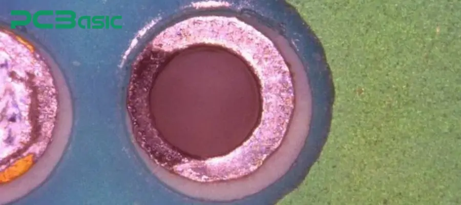
The "black pad" on the PCB refers to a common and serious defect that occurs during the ENIG surface treatment process.
According to normal procedures, the nickel layer and the gold layer should evenly cover the copper surface to provide protection and good solderability for the solder pads. However, when hyper-corrosion occurs during the ENIG process, the nickel layer beneath the gold layer will become significantly darker, blackened, brittle, and accompanied by abnormal chemical composition, thus forming the so-called "black pads".
This defect has a significant impact on the solderability of the solder pads, causing the solder joints to become brittle, poor in wetting, and the connection strength to decrease, and even leading to long-term electrical failure of the product.
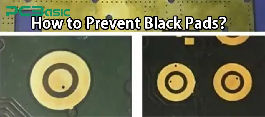
A PCB with black pads typically shows:
dark, dull, or “pepper-like” black pads
streaks along nickel grain boundaries
uneven gold surface
solder that refuses to wet the pad
brittle, grainy solder joints
As shown in the figure,
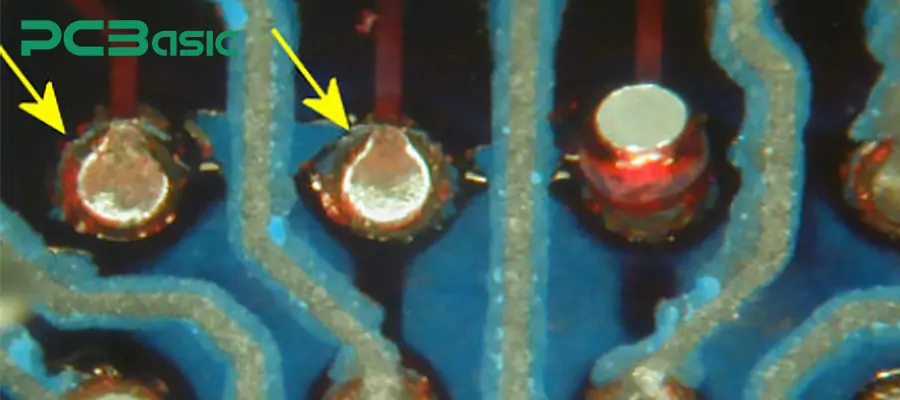
In many cases, black pads are difficult to detect with the naked eye. We usually need to conduct cross-sectional analysis or use professional imaging equipment to detect black pads. The presence of black pads indicates that the nickel layer has undergone corrosion. If cracks or micro-cracks appear on the ENIG surface of the black spot, it indicates that the nickel layer has become even more brittle.
This is because the black pad is actually a metallurgical breakdown at the solder joint interface. As we mentioned earlier, this defect is particularly prone to occur on the circuit boards with ENIG surface treatment. And the ENIG process itself is widely used in high-reliability scenarios. In such cases, the harm of the black pad becomes more prominent. Its severity mainly manifests in four reliability threats:
1. Solder point embrittlement: Loss of mechanical durability
The black coating can cause abnormal reactions between the corroded nickel surface and the molten solder. At this point, what is formed is no longer the tough nickel-tin intermetallic compound (IMC, such as Ni₃Sn₄), but rather porous and fragile intermetallic compounds (such as Ni₃P or nickel oxide). These brittle layers lack flexibility, and even minor environmental stresses can trigger microcracks, leading to a decrease in the strength of the solder joint.
2. Open circuit failure: Complete failure of electrical connection
The black pad will disrupt the solder wetting process. If it is a "partial non-wetting" situation (where the solder forms beads instead of spreading out), intermittent electrical connections will be formed; even complete open circuits may occur. If the solder is unable to adhere to the pad consistently, it will result in power or signal interruption for the component.
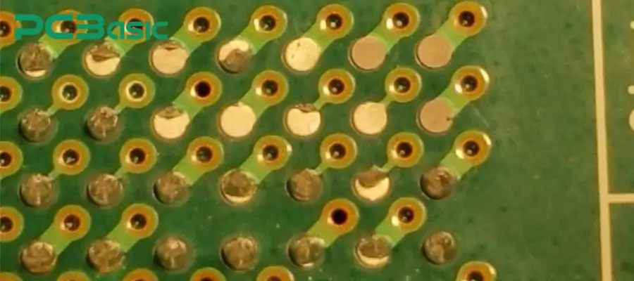
3. Potential Field Failures
The concealment of black pad defects lies in the fact that they often lead to potential failures. That is, the circuit board passes the factory inspections (such as appearance checks, continuity tests) and is deemed qualified, but it fails prematurely after being put into use. This is a catastrophic situation for industries that rely on the reliability of ENIG.
4. High costs: Re-work, Scrap
ENIG circuit boards are mostly used in high-value products (such as smart phones, industrial controllers), and defects in the black pad can directly result in huge economic losses.
The formation of black pad is caused by abnormal chemical reactions and improper process control. The main causes are as follows:
1. Overcorrosion of the nickel layer during the gold plating stage
In the ENIG process, if the gold immersion bath is too corrosive, contaminated by impurities, or if the process control is improper (such as unstable temperature and chemical concentration), the nickel layer will corrode sharply. Then, this excessive corrosion will form porous, corroded-like nickel "spikes" on the pad surface, which directly leads to the formation of black pads.
2. The phosphorus content in the nickel layer is too high.
The phosphorus concentration in the chemical nickel plating bath directly affects the structure of the nickel layer. If the plating bath produces a high-phosphorus nickel layer (with a phosphorus content typically exceeding about 12%), this layer will inherently become brittle and porous. This fragile structure will accelerate corrosion during the gold plating stage. Moreover, since the chemical substances in the gold plating bath are prone to penetrating the gaps in the nickel layer, this creates ideal conditions for the formation of the black pad.
3. The ENIG process control is improper throughout the entire procedure.
The formation of black pads is often the result of poor process management. The key mistakes include:
Abnormal pH values in the nickel or gold baths
Inappropriate gold layer thickness
Old age of the electroless plating baths
Insufficient rinsing after nickel plating
Excessive residence time in the gold bath
These mistakes will disrupt the delicate balance of the ENIG reaction, making the formation of black pads inevitable.
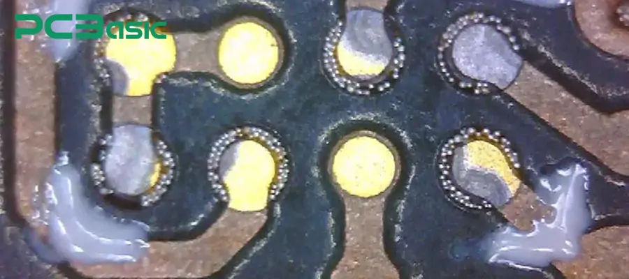
4. Insufficient activation of the pre-coated surface
Surface activation is a crucial pretreatment step to ensure uniform deposition of the nickel layer. If the activation is incomplete or uneven, the subsequently deposited nickel layer will exhibit blemishes - existing in the weak areas with poor corrosion resistance. These weak points will corrode first during the gold plating stage, resulting in uneven gold layer coverage and ultimately forming a black padoloration.
5. Excessive Cleaning or Use of Abrasive Stripping Pads
Pre-cleaning of the solder pads is an essential step in the surface pretreatment process. However, overdoing the cleaning can have the opposite effect. Using abrasive cleaning materials or applying excessive pressure during cleaning can scratch or damage the base material of the solder pads. These tiny scratches will create fine cracks, allowing corrosive chemicals in the nickel or gold slots to accumulate and accelerate local corrosion.
In conclusion, the black pads are the direct consequence of the imbalance in the ENIG chemical reaction and improper process control.
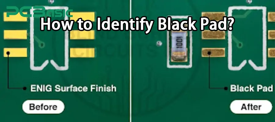
1. First of all, we can conduct a preliminary screening through visual inspection. Observe:
Is the color of the pads abnormal? Black pads may show local or overall blackening, greying, or dark brown pads, and the color lacks luster and cannot be removed by wiping.
Wetting marks of solder: If there are "dimpled" soldering beads on the pads after soldering, or some areas are not covered by solder, or there is black staining around the edges of the solder joints, it is likely caused by the poor wetting of the black pads.
Batch regularity: Black pads often appear in batches. If multiple pads in the same batch of PCB show the same color abnormalities or wetting problems, and they are concentrated in specific areas (such as boards processed in the same plating bath), then it is highly likely that the black pads are the cause.
2. Quickly determine through physical and simple chemical tests.
Cleaning test: Soak a cotton swab in anhydrous ethanol or isopropyl alcohol, and gently wipe the abnormal area of the solder pad. If it cannot be wiped off and there are no obvious scratches on the solder pad surface, the probability of a black pad (black pad) is extremely high.
Tape adhesion test: Stick a high-strength adhesive tape and quickly peel it off. The black pad area will together with the gold layer and the corroded nickel layer fall off, revealing the black corroded substrate beneath.
Wetting test: Use standard solder wire to conduct manual soldering on the solder pad. Observe the solder spreading speed. The solder in the black pad area will quickly shrink into a ball shape, or it will not adhere at all.
3. Use professional instruments for analysis and achieve precise confirmation.
Metallographic sectioning and microscope observation: Cut the cross-section of the solder pad using a slicing machine and observe it with a metallographic microscope - the black pad (black pad) will show a porous nickel layer, corrosion cavities, or a black corrosion layer between the gold layer and the nickel layer.
EDS: Test the elemental composition of the solder pad. For the black pad (ENIG), there will be abnormal reduction in nickel content, increased oxygen content (oxidation corrosion), or locally higher phosphorus content.
XRF: Rapidly detect the thickness of the gold layer and the state of the nickel layer. The black pad area often accompanies uneven thickness of the gold layer (local thinning) or abnormal thickness of the nickel layer.
1. Strictly control the parameters of the ENIG plating bath (core prevention)
2. Standardize the pretreatment and post-treatment processes
3. Optimize soldering and storage conditions
4. Strengthen process monitoring and quality traceability
5. Alternative Process Selection (High-risk Scenarios)
For high-reliability products that have zero tolerance for black pads (such as aerospace and medical equipment), the ENIG process can be replaced with ENEPIG.
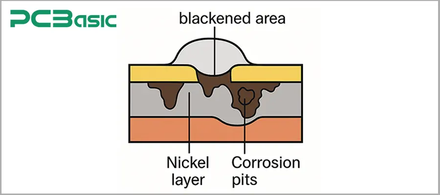
The formation of black pad is fundamentally due to the uncontrolled corrosion of the nickel layer in the ENIG process. The corrosion of the nickel layer is not a single reaction but a sequential process of "dissolution - oxidation - brittleness".
After the normal replacement reaction in the gold plating bath becomes out of control, the nickel layer undergoes excessive dissolution and reacts with oxygen and phosphorus to form black porous corrosion products such as NiO, Ni₂O₃, and Ni₃P. These products accumulate at the gold-nickel interface, destroying the metallurgical bonding force between the two, causing the gold layer to float, the surface of the pad to turn black and lose its solder wetting ability. This is the exclusive formation mechanism of black pad ENIG.
Excessive corrosion of the nickel layer is the most critical factor driving the formation of the black pad. The key differences and specific characteristics between this and normal corrosion are as shown in the table below:
|
Comparison Dimension |
Normal Nickel Corrosion (Benign Reaction) |
Nickel Hyper-Corrosion (Black Pad Trigger) |
|
Dissolution Thickness |
<0.1μm, only the surface layer participates in the reaction |
>0.5μm, deep nickel layer is eroded |
|
Reaction Rate |
Slow, automatically terminates after gold layer deposition |
Fast, not inhibited by gold layer coverage |
|
Product State |
No obvious corrosion products, clear gold-nickel interface |
A large amount of black corrosion products (NiO, Ni₃P), blurred interface |
|
Gold Layer Condition |
Uniformly adhered, tightly bonded to the nickel layer |
Partially lifted, cracked, with extremely poor adhesion |
|
Pad Appearance |
Uniform bright gold color, no blackening |
Local or overall blackening, dull luster |
|
Soldering Performance |
Solder wets quickly and spreads evenly |
Solder beads up, fails to wet, prone to open circuits |
In short, hyper-corrosion of the nickel layer is the "key driver" behind the formation of the black pad.
Black pads are a common defect in ENIG circuit boards and are quite difficult to detect. By reading this article, you will be able to understand the formation mechanism, detection methods and preventive measures of black pads. These will greatly contribute to enhancing the reliability of PCBs and avoiding high costs.
 About PCBasic
Time is money in your projects – and PCBasic gets it. PCBasic is a PCB assembly company that delivers fast, flawless results every time. Our comprehensive PCB assembly services include expert engineering support at every step, ensuring top quality in every board. As a leading PCB assembly manufacturer, we provide a one-stop solution that streamlines your supply chain. Partner with our advanced PCB prototype factory for quick turnarounds and superior results you can trust.
1. Can Black Pad be repaired?
In some cases, the repair can be achieved by removing the original ENIG coating and re-plating with nickel and gold. However, if the nickel layer has suffered severe "hyper-corrosion", most PCBs cannot be effectively repaired.
2. How much gold thickness is safe?
It is generally believed that a gold thickness of 2 to 5 microinches is a relatively safe and common range.
3. Does reflow temperature worsen Black Pad defects?
High temperature itself does not cause black spots, but it makes the existing defects more obvious. Specifically, this manifests as:
Accelerate the brittle fracture of solder joints
Make it easier to expose the poor formation of nickel-silicon intermetallic compounds (IMC)
More likely to experience open circuits during thermal cycling

Assembly Enquiry
Instant Quote
Phone contact

+86-755-27218592
In addition, we've prepared a Help Center. We recommend checking it before reaching out, as your question and its answer may already be clearly explained there.
Wechat Support

In addition, we've prepared a Help Center. We recommend checking it before reaching out, as your question and its answer may already be clearly explained there.
WhatsApp Support

In addition, we've prepared a Help Center. We recommend checking it before reaching out, as your question and its answer may already be clearly explained there.