Global high-mix volume high-speed PCBA manufacturer
9:00 -18:00, Mon. - Fri. (GMT+8)
9:00 -12:00, Sat. (GMT+8)
(Except Chinese public holidays)
Global high-mix volume high-speed PCBA manufacturer
9:00 -18:00, Mon. - Fri. (GMT+8)
9:00 -12:00, Sat. (GMT+8)
(Except Chinese public holidays)
HomePage > Blog > Knowledge Base > Lead-Free PCB Assembly: Guide to RoHS-Compliant PCBA Manufacturing
With the global attention paid to the environmental impact of electronic waste continue to rise, countries worldwide have successively introduced environmental regulations to restrict the use of harmful substances in electronic products. The global electronics industry has begun a large-scale transformation towards environmentally friendly manufacturing, and lead-free PCB assembly has also become a mainstream trend in this context.
After the enforcement of the EU RoHS directive, global consumer electronics brands have adopted the same standard. Coupled with the continuous growth of the market demand for green electronic products, lead-free PCB assembly services have become the basic requirement for various electronic products to enter the international market. Therefore, understanding how lead-free PCB assembly works, the main differences between it and traditional leaded solder, and the impact of material selection, temperature management and process control on product performance have all become basic professional capabilities.
This guide will take you to quickly understand the key materials, process requirements, core purposes of the RoHS directive, and the restricted substances list of SMT lead-free PCB assembly, and explain when manufacturing durable, reliable and truly environmentally compliant electronic products, engineering details and practical experience that need attention.
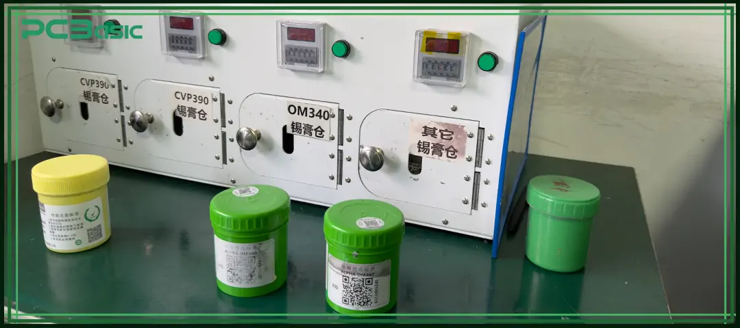
Lead-free PCB assembly refers to the assembly of circuit boards using lead-free solder, RoHS-compliant PCB substrates, and electronic components that meet environmental protection standards.
Most circuit boards in the past were assembled using traditional leaded solder (Sn/Pb alloys). This solder has good solderability, strong wettability and a low melting point. However, as lead is harmful to both the environment and human health, environmental protection regulations around the world have begun to restrict lead-containing materials, so lead-free PCB assembly has gradually become mainstream.
In lead-free PCB assembly, solder joints are formed using other metal alloys. Many engineers often ask: What is lead-free solder made of?
Common lead-free solder formulations include:
• SAC305 (Sn96.5/Ag3.0/Cu0.5)
• SAC405
• Sn/Cu (for cost-sensitive applications)
• Sn/Bi (better ductility, suitable for special applications)
The melting points of these lead-free solders are typically around 217 to 220°C, significantly higher than the 183°C of traditional Sn/Pb solders. Therefore, higher soldering temperatures will significantly affect the selection of PCB substrates, the setting of reflow soldering temperature profiles, the thermal tolerance of components, and the long-term reliability of the products.
Regardless of the product type, the materials and processes used in lead-free PCBs must comply with the requirements of the RoHS regulation to ensure that all harmful substances in the materials are controlled within the allowable range.
RoHS (Restriction of Hazardous Substances) is an environmental regulation introduced by the European Union. Its core purpose is very simple: to reduce the pollution of electronic waste to the environment and protect people from exposure to toxic substances.
It requires strict control over hazardous components in electronic products to prevent pollution of soil, water sources and air, and also to reduce the risk of workers being exposed to harmful chemicals during the manufacturing and recycling processes. In addition, RoHS also makes electronic waste easier to be safely recycled and promotes the global electronics industry to gradually use safer and more environmentally friendly materials.
Nowadays, whether in Europe, the United Kingdom, some states in the United States, or in the global mainstream consumer electronics market, compliance with RoHS has become a necessary condition for products to enter the market, rather than just an optional advantage.
RoHS currently imposes restrictions on the following 10 substances:
|
Maximum Limit |
|
|
Lead (Pb) |
0.1% |
|
Mercury (Hg) |
0.1% |
|
Cadmium (Cd) |
0.01% |
|
Hexavalent Chromium (Cr6+) |
0.1% |
|
PBB |
0.1% |
|
PBDE |
0.1% |
|
DEHP |
0.1% |
|
BBP |
0.1% |
|
DBP |
0.1% |
|
DIBP |
0.1% |
Together, they form the global foundation for sustainable electronics manufacturing.
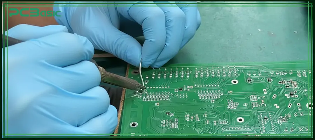
Since lead-free solder requires a higher temperature during reflow soldering, the substrate used for lead-free PCB assembly must have better thermal resistance.
High Tg and high Td materials such as IS410, IS420, FR408HR, R370HR, as well as some high-performance epoxy systems, are commonly used as lead-free substrates. These materials have all passed UL certification and can withstand soldering temperatures ranging from 260°C to 300°C in SMT lead-free PCB assembly without delamination, warping or thermal failure.
The commonly used surface finishes for lead-free PCBs include ENIG, ENEPIG, immersion silver, immersion tin, OSP, and HASL lead-free PCB assembly, which is common in lighting products, as well as hard gold and soft gold finishes. These surface treatments have good compatibility with modern lead-free solders, can provide stable solderability, oxidation resistance, and maintain a long storage life, and are very suitable for the production requirements of lead-free products.
The traditional HASL with leaded solder has been explicitly prohibited by RoHS due to the use of leaded solder. Any surface finish that may exceed the limits of RoHS hazardous substances cannot be used in the manufacturing of lead-free PCBs, either.
Time is money in your projects – and PCBasic gets it. PCBasic is a PCB assembly company that delivers fast, flawless results every time. Our comprehensive PCB assembly services include expert engineering support at every step, ensuring top quality in every board. As a leading PCB assembly manufacturer, we provide a one-stop solution that streamlines your supply chain. Partner with our advanced PCB prototype factory for quick turnarounds and superior results you can trust.
Leaded solder is a traditional solder alloy composed of tin and lead, with the most common composition being Sn63/Pb37. This solder has the advantages of a low melting point (183°C), good wettability, strong fluidity, and a stable solder joint appearance. Therefore, it was almost the standard material for all PCB assemblies over the past few decades.
Due to its low operating temperature, wide soldering window, and minimal thermal stress on components and PCBs, leaded solder is very easy to solder and has a high tolerance rate. Therefore, it was regarded as one of the most stable and effective types of solder.
However, lead is a harmful heavy metal. When electronic waste is recycled or decomposed at high temperatures, it will seep into the environment, causing pollution to human health and the ecosystem. Therefore, after the implementation of the RoHS regulation, leaded solder has been widely restricted and gradually replaced by lead-free solder.
|
Feature |
Leaded Solder |
Lead-Free Solder |
|
Melting Point |
183°C |
217–220°C |
|
Reliability |
Good |
Excellent (creep resistance & fatigue) |
|
Environmental Impact |
Toxic |
Eco-Friendly |
|
Oxidation |
Lower |
Higher (requires flux optimization) |
Despite its higher melting point, lead-free PCB assembly now matches or exceeds Sn/Pb reliability in most applications.
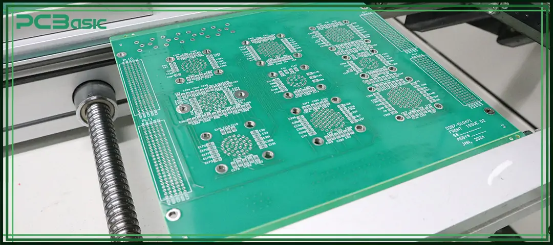
To achieve highly reliable lead-free PCB assembly, the following points must be given key attention during the manufacturing process:
Lead-free products may undergo high-temperature cycles ranging from -45 °C to +145°C during operation, with the total number of cycles even exceeding 2,000. Therefore, high-TD PCB substrates and precise reflow soldering temperature control are crucial for maintaining reliability.
Excessively high reflow soldering temperatures will accelerate the growth of IMC, making the solder joints brittle and reducing reliability. In SMT lead-free PCB assembly, controlling the thickness of IMC by optimizing the reflow profile is an important stage to ensure the strength of solder joints.
For high-reliability scenarios such as handheld devices and automotive electronics, the following measures can significantly enhance the mechanical strength of solder joints:
• Underfill
• Corner bonding
• Optimized fillets
These reinforcement techniques help to enhance the long-term stability of lead-free assembled products in shock and vibration environments.
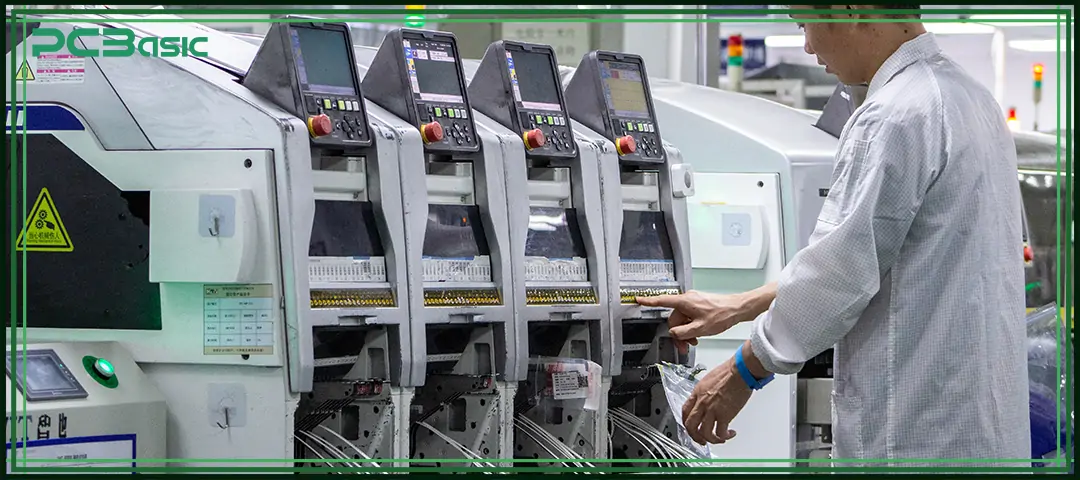
PCBasic runs 100% lead-free SMT and THT lines to prevent any chance of leaded solder contamination. All materials—laminates, solder pastes, components, coatings, and packaging—meet RoHS and REACH requirements and are verified with strict XRF testing.
Our facilities comply with ISO 9001, IATF 16949, ISO 14001, ISO 45001, and UL, and all assemblies follow IPC-A-610 Class 2/3 standards. This ensures consistent quality across automotive, industrial, medical, and consumer electronics.
PCBasic engineers fine-tune every step of lead-free PCB assembly, from reflow profiling and SAC alloy selection to nitrogen reflow and DFM/DFX review, ensuring strong solder joints and reliable long-term performance.
We offer complete lead-free PCB assembly services, including PCB fabrication, lead-free SMT, wave soldering, AOI/X-Ray/SPI inspection, ICT/FCT testing, conformal coating, firmware programming, and box-build assembly. This reduces lead time and keeps the entire process consistent.
Every BOM is checked for RoHS compliance. Non-compliant or Sn/Pb-only components are replaced with RoHS-certified alternatives from reliable manufacturers and distributors.
PCBasic’s lead-free assemblies perform well under high thermal cycling, vibration, and mechanical shock, making them suitable for LED lighting, automotive electronics, industrial control, and medical devices.
With efficient SMT lines, MES/ERP traceability, and a strong supply chain, PCBasic delivers high-quality China lead-free PCB assembly with competitive pricing for both prototypes and mass-production runs.
With the continuous development of the global electronics manufacturing industry towards sustainability and environmental protection, lead-free PCB assembly has become a common industry standard. The shift from traditional leaded solder to modern SAC system solder has led to significant improvements in the safety, reliability and recyclability of electronic products.
Whether you are developing lighting products using HASL lead-free PCB assembly, IoT devices using SAC solder, or industrial electronic products pursuing high reliability, choosing a manufacturing method that complies with RoHS requirements can ensure that your products are safer, more globally competitive, and well-prepared for the future market.
1. Are lead-free solder joints as reliable as Sn/Pb?
Yes. Modern lead-free solder alloys like SAC305 provide excellent fatigue, creep, and thermal cycling performance—often better than leaded solder.
2. Does lead-free PCBA cost more?
Today, the cost difference is minimal. With mass adoption and mature processes, China's lead-free PCB assembly pricing is now nearly identical to Sn/Pb assembly.
3. Do lead-free boards require longer production time?
Not significantly. While the lamination cycle is slightly longer due to high-Td materials, overall lead time is nearly identical.
4. How do factories prevent cross-contamination with lead?
• Separate production lines
• Dedicated solder equipment
• XRF material analysis
• Strict warehouse control
5. What’s the best surface finish for lead-free PCBs?
ENIG is the most versatile. For LEDs, HASL lead-free LED PCB assembly is also common. OSP and Immersion Silver are suitable for cost-sensitive builds.
6. How to verify RoHS compliance from a Chinese EMS provider?
Request:
• RoHS Certificate of Compliance
• XRF reports
• IPC-A-610 / J-STD-001 process documentation
• UL laminate verification
7. What solder alloy is best for my application?
• SAC305 for general use
• Sn/Cu for wave soldering
• Sn/Bi for low-temperature assemblies
• Low-silver SACX for cost reduction
8. Can lead-free PCBs handle high-power or automotive use cases?
Yes—when using high-Td laminates, controlled reflow profiles, and reinforced solder joints, lead-free PCB assembly is suitable for EV, industrial, and aerospace applications.

Assembly Enquiry
Instant Quote
Phone contact

+86-755-27218592
In addition, we've prepared a Help Center. We recommend checking it before reaching out, as your question and its answer may already be clearly explained there.
Wechat Support

In addition, we've prepared a Help Center. We recommend checking it before reaching out, as your question and its answer may already be clearly explained there.
WhatsApp Support

In addition, we've prepared a Help Center. We recommend checking it before reaching out, as your question and its answer may already be clearly explained there.