Global high-mix volume high-speed PCBA manufacturer
9:00 -18:00, Mon. - Fri. (GMT+8)
9:00 -12:00, Sat. (GMT+8)
(Except Chinese public holidays)
Global high-mix volume high-speed PCBA manufacturer
9:00 -18:00, Mon. - Fri. (GMT+8)
9:00 -12:00, Sat. (GMT+8)
(Except Chinese public holidays)
HomePage > Blog > Knowledge Base > FPGA Board: The Complete Guide to Design, Layout, and Manufacturing
In modern electronics and embedded systems, FPGA boards have become a very important core hardware component. Whether you are engaged in artificial intelligence (AI), industrial automation, Internet of Things (IoT) devices, or high-performance computing (HPC), FPGA boards can achieve functions and flexibility that traditional solutions, such as microcontrollers or ASICs, cannot.
So, what exactly makes an FPGA board so special? How is FPGA programming implemented? What exactly are the differences between Field Programmable Gate Array (FPGA) and ordinary logic chips? If you have an idea, how can you make a reliable, scalable and mass-production-suitable FPGA development board?
This guide will systematically answer these common questions and also introduce more related knowledge. We will combine industry practice and practical experience to provide you with a detailed explanation of the entire process of FPGA board design, layout and manufacturing, from the core architecture, design process to mass production and manufacturing of the FPGA board.
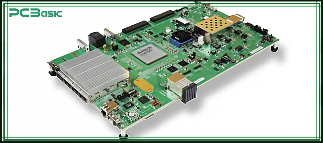
The core of the FPGA board is a Field Programmable Gate Array (FPGA). It is a very powerful and flexible chip. After the chip is manufactured, users can configure and modify the internal digital logic of the chip through FPGA programming according to their own needs. Unlike microcontrollers that can only run fixed programs and have a fixed hardware structure, FPGAs can repeatedly update their hardware configurations to achieve different functions.
The FPGA board, also known as the FPGA development board, is a complete hardware platform. It not only contains Field Programmable Gate Array (FPGA), but also integrates memory, voltage regulators and connectors. Some also come with dedicated peripherals or embedded processors, which can be directly used for direct application development.
FPGA boards are widely used in industries like aerospace, telecommunications, automotive, medical devices and machine learning. Its greatest advantage lies in its flexibility and multi-functionality. Through FPGA programming, engineers can flexibly customize hardware according to project requirements to achieve rapid prototyping, repeated iterations, and parallel processing tasks that traditional CPUs cannot efficiently complete.
When choosing your FPGA board, first figure out the main types available on the market. FPGA boards can generally be divided into two types:
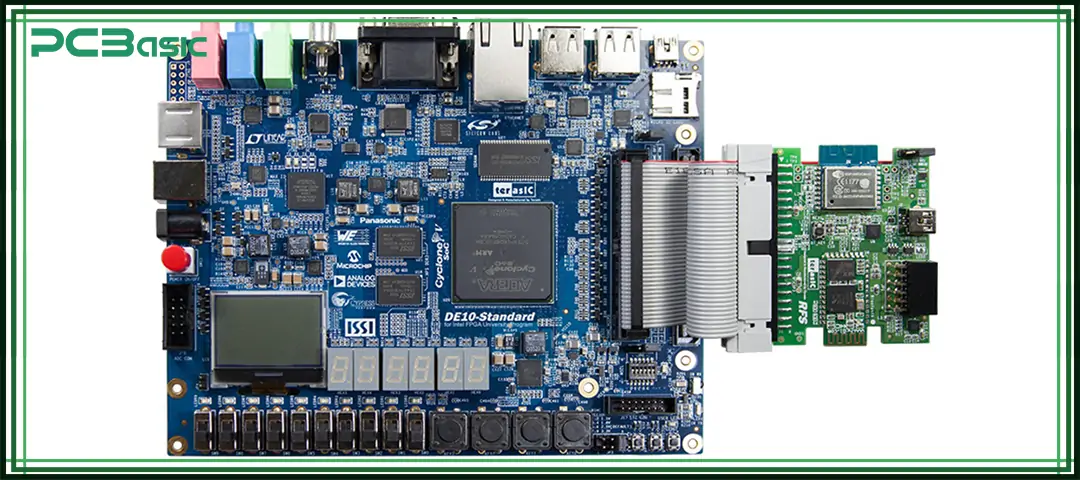
The first is commercial off-the-shelf (COTS) FPGA board (FPGA board). This type of FPGA development board is produced in advance by mainstream manufacturers and can be directly used for prototype design or proof-of-concept work. COTS FPGA boards are suitable for learning, rapid prototyping, academic projects and initial development. Its main advantages are: quick market launch, built-in programming and debugging functions, and a wide range of choices, including both low-cost models and high-performance versions.
The second is custom FPGA board. If you are going to produce commercial products, engage in mass production, or have special requirements for your project, then you need to customize an FPGA board. The common reasons for choosing custom FPGA boards include: special customization of size or shape, the need for high-speed I/O or dedicated connectors, the hope to achieve advanced functions that standard FPGA development boards do not have, cost optimization based on mass production, and full control over design and supply chain.
These two types of FPGA boards each have their applicable scenarios. When choosing, you should decide based on your actual needs.
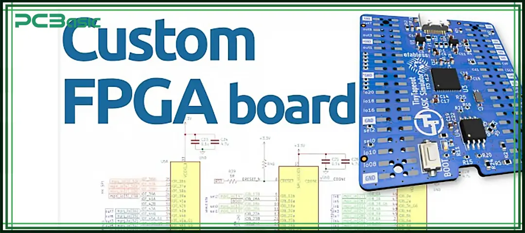
Whether you choose a COTS or a custom FPGA board, you should consider the following factors:
• Project lifecycle: Does the board require long-term support?
• Required interfaces and number of I/Os: How many signals are needed? What are the operating voltage levels?
• Power consumption and thermal requirements
• Performance targets: speed, logic resources, and memory capacity
• Budget and time constraints
Choosing the right FPGA board (FPGA board), whether for prototyping or mass production, is the key to project success.
 About PCBasic
Time is money in your projects – and PCBasic gets it. PCBasic is a PCB assembly company that delivers fast, flawless results every time. Our comprehensive PCB assembly services include expert engineering support at every step, ensuring top quality in every board. As a leading PCB assembly manufacturer, we provide a one-stop solution that streamlines your supply chain. Partner with our advanced PCB prototype factory for quick turnarounds and superior results you can trust.
A modern FPGA board not only has a Field Programmable Gate Array (FPGA) but also integrates many key components. The following are the main components:
The core of an FPGA board is the FPGA chip. The chip contains the following modules inside:
• Configurable Logic Blocks (CLBs): These are the fundamental units for FPGAs to implement various logic functions.
• Programmable Interconnects: Used to connect different logic blocks, they can achieve any digital circuit structure.
• I/O Blocks: These interfaces are responsible for data communication with external devices, such as LVDS, LVCMOS, and differential signals.
• Memory Elements: These include Block RAM, distributed RAM, and some even have memory controllers.
• Clock Management: It includes PLLs and DLLs, which are used to generate and manage multiple clock domains to achieve precise clock distribution.
An FPGA board requires multiple power supplies, such as core circuits, I/O circuits, and auxiliary modules. A Voltage Regulator and a Decoupling Capacitor will be specially placed on the board. This ensures a stable power supply and low noise and prevents voltage fluctuations from affecting the normal operation of the circuit.
FPGA programming is generally implemented through interfaces such as JTAG and SPI. Many FPGA boards also come with a USB downloader, which can be directly connected to a computer for burning and debugging, making it very convenient for developers to get started quickly.
Many FPGA development boards are equipped with external storage chips such as SDRAM and Flash, which are used to store startup files, data or as cache.
High-density connectors (such as FMC, PMOD or custom sockets) enable FPGA boards to be easily expanded, allowing for the installation of various sensors, screens or custom functional modules to meet the requirements of different projects.
Some advanced FPGA boards also integrate microprocessors, ADC/DAC (analog-to-digital/digital-to-analog converters), Ethernet PHY chips or Wireless interfaces. This way, complex embedded systems can be directly built without the need for additional sub-boards, which not only saves space but also enhances integration.
Designing a PCB for an FPGA board needs to be carried out in stages, and each step should take into account both creativity and engineering specifications. The specific process is as follows:
System Specification and Schematic Design
First of all, you need to clarify what goals your designed FPGA board aims to achieve and what functions it requires. Select the appropriate FPGA chip and record in detail all interfaces, I/O ports, power supply and storage requirements. The schematic diagram should be drawn concisely and clearly. Pin allocation should be clear. If there are unused FPGA pins, it is recommended to lead them out to the pin header for convenient subsequent debugging.
PCB Stackup and Layer Planning
Modern FPGA boards typically require at least 4 to 6 layers to ensure signal integrity, power distribution, and EMI/EMC performance. If it is a high-speed design, it may require 8 layers or even more.
The signal layer and the power/ground plane layer are alternately arranged (such as signal-ground-signal-power).
Impedance control for high-speed signals should be planned in advance.
Ensure that the power supply layer and the stratum are continuous and uninterrupted.
Component Placement
Arrange key components such as FPGA chips, decoupling capacitors, memory chips, and connectors in a reasonable layout. High-speed signals should take the shortest route as much as possible. Put the related components together. When designing, consider heat dissipation in advance, such as reserving the positions for heat sinks or thermal vias.
Routing and Signal Integrity
High-speed signal routing is extremely crucial:
Differential signals must be length-matched.
Avoid right angles and try to use 45-degree or curved routing as much as possible.
Maintain consistent impedance throughout the process and minimize unnecessary branches.
The clock and reset signal traces should be neat to minimize skew and jitter.
Power Distribution Network (PDN) Design
The power supply traces should be wide enough, or a power layer can be used directly. The decoupling capacitor should be placed as close as possible to the power pins of the FPGA. Power supply filtering requires the combination of large capacitors and ceramic capacitors to take into account noise suppression at different frequencies.
Clock Distribution
The clock tree structure should be reasonably designed to reduce the skew of the clock signal. Complex FPGA boards can use a dedicated layer of clock routing or adopt shielded lines to reduce interference.
Documentation and Version Control
Interface tables, schematics, and pin assignment documents must all be archived and managed in a version control system. Documentation should be clear and accurate, which is especially important for collaborative development or multi-board system projects.
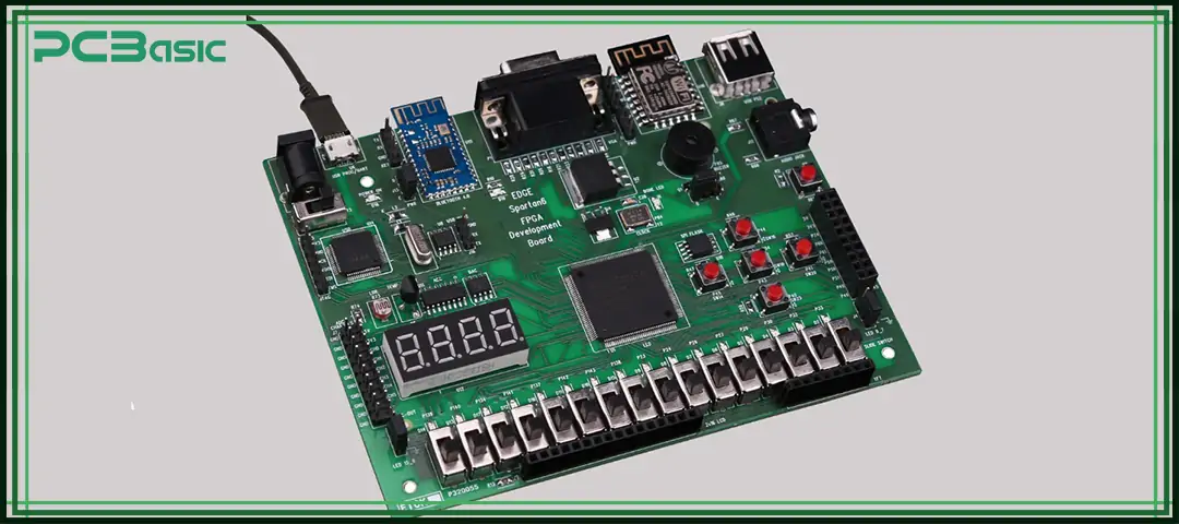
When designing an FPGA board, every stage requires the right tools and technologies. The details are as follows:
Commonly used FPGA board (FPGA board) design software includes:
• Altium Designer: Supports advanced routing, 3D visualization, and is well-suited for FPGA-related development.
• Cadence Allegro: Very suitable for designing large and complex FPGA boards, with strong constraint management capabilities.
• Mentor Graphics PADS: Integrates signal integrity analysis and pin optimization functions.
• KiCad: Open-source software, ideal for small FPGA development board projects.
For high-speed FPGA boards (FPGA board), you need specialized analysis tools:
• Ansys SIwave
• Cadence Sigrity
• Mentor HyperLynx
• Keysight ADS
These tools help you identify issues such as impedance mismatches, crosstalk, and power plane resonances.
Modern FPGA boards (FPGA board) have high requirements for thermal management. Common tools include:
• Ansys Icepak
• 6SigmaET
• FloTHERM
These software tools help you analyze and optimize PCB heat dissipation.
For FPGA programming, simulation, and synthesis, the following tools are commonly used:
• Xilinx Vivado
• Intel Quartus Prime
• Microsemi Libero SoC
• Lattice Diamond
These tools can generate configuration files (bitstreams) from HDL code that can be used directly by the FPGA board.
Nowadays, many design workflows require PCB engineers and FPGA programming engineers to collaborate. Co-design tools can support pin swapping, interface optimization, and rapid design iteration, improving overall efficiency.
The FPGA board is the core hardware of modern digital systems. It features extremely high flexibility, powerful parallel processing capabilities and excellent performance. To do a good job in the design of an FPGA board, you need to understand the core architecture of the field programmable gate array, and also master the circuit board layout, signal integrity control and manufacturing process. The realization of high-quality FPGA boards is inseparable from solid knowledge, precise engineering methods and appropriate design tools.
As long as you follow the best practices in this guide, you can confidently complete the design, prototype development and mass production manufacturing of the FPGA board, ensuring that the developed FPGA development board is reliable enough to cope with various application challenges.
Q1: When should I choose a custom FPGA board vs. a standard dev board?
A: Choose a standard FPGA development board (COTS) for learning, prototyping, or when your needs match off-the-shelf features. Opt for a custom FPGA board if you need a specific size, I/O, performance, or cost optimization, especially for production.
Q2: What’s the minimum PCB layer count for a modern FPGA board?
A: For basic FPGA boards, 4 layers is the minimum. Most high-speed, reliable designs use 6–10+ layers to ensure solid power/ground planes and impedance-controlled signals.
Q3: How to avoid common design mistakes?
A: Always document pin assignments and interfaces, use adequate decoupling, verify stackup for signal integrity, and simulate power delivery. Use version control for all design files and interface tables.
Q4: How to ensure signal and power integrity for high-speed FPGAs?
A: Use matched impedance routing, differential pairs, minimize trace lengths, and provide robust power/ground planes. Simulate with SI/PI tools and follow best practices for decoupling and plane layout.
Q5: What are the best tools for FPGA board design?
A: Industry leaders include Altium Designer, Cadence Allegro, Mentor Graphics PADS, and KiCad for PCB; Xilinx Vivado and Intel Quartus Prime for FPGA programming; and tools like Sigrity and HyperLynx for SI/PI analysis.

Assembly Enquiry
Instant Quote
Phone contact

+86-755-27218592
In addition, we've prepared a Help Center. We recommend checking it before reaching out, as your question and its answer may already be clearly explained there.
Wechat Support

In addition, we've prepared a Help Center. We recommend checking it before reaching out, as your question and its answer may already be clearly explained there.
WhatsApp Support

In addition, we've prepared a Help Center. We recommend checking it before reaching out, as your question and its answer may already be clearly explained there.