Global high-mix volume high-speed PCBA manufacturer
9:00 -18:00, Mon. - Fri. (GMT+8)
9:00 -12:00, Sat. (GMT+8)
(Except Chinese public holidays)
Global high-mix volume high-speed PCBA manufacturer
9:00 -18:00, Mon. - Fri. (GMT+8)
9:00 -12:00, Sat. (GMT+8)
(Except Chinese public holidays)
HomePage > Blog > Knowledge Base > Wire Bonding Explained – A Comprehensive Guide
In microelectronics, wire bonding is one of the major processes. For many years, manufacturers have used this technique for two purposes. It makes a seamless electrical and mechanical connection between tiny semiconductor dies and their external packaging.
There is tight competition from alternatives such as flip chips and advanced 3D packaging. However, wire bonding dominates as the top-level interconnect technology.
For example, it is responsible for over 75% of all die to package connections globally.
To understand IC wire bonding, PCB wire bonding, and semiconductor wire bonding, you need to understand the basics of the wire bonding process, bond wire materials, and future trends.
Subsequently, this article provides a comprehensive examination of wire bonding, focusing on:
• Techniques
• Materials
• Applications
• Cost
• Common Issues
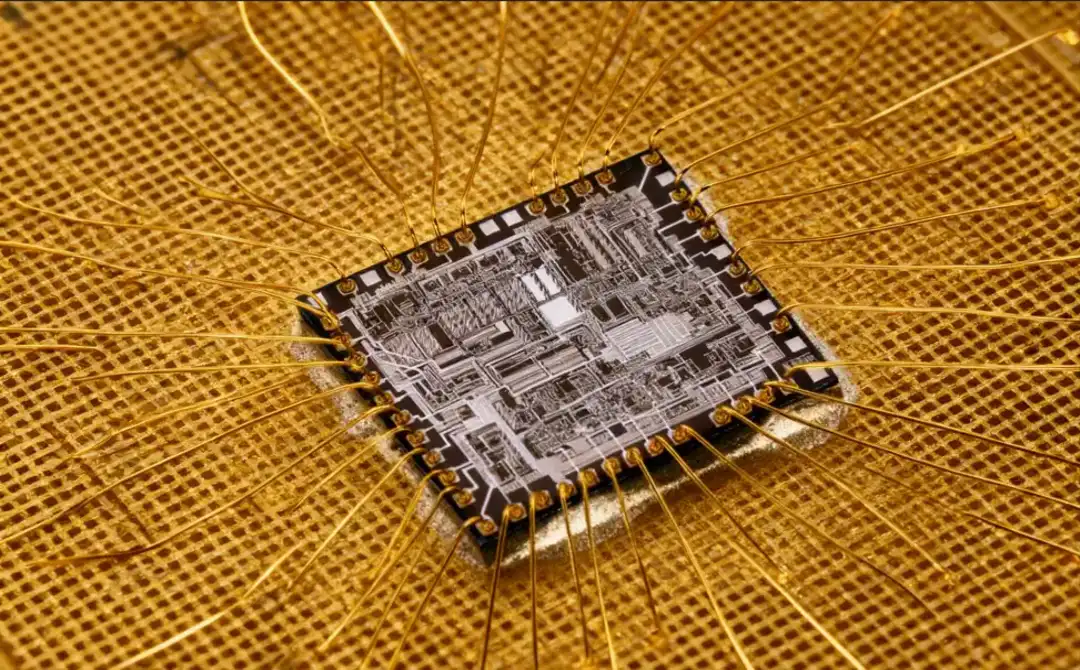
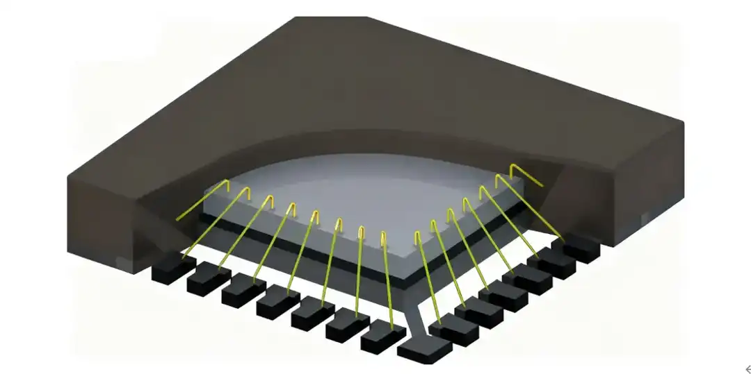
Wire bonding is the process by which semiconductor devices are electrically connected to a package, substrate, and printed circuit board. This process incorporates fine wires. These bonding wires are generally made from gold, aluminum, and copper. These are attached using pressure combined with heat and ultrasonic energy.
The main advantages of wire bonding include:
Wire Bonding is Versatile
It accommodates a wide array of materials, package types, and device geometries, making it suitable for virtually any application.
Easily Scalable
It supports high-volume IC wire-bonding production while also being viable for low-volume, specialized projects.
Reliable Manufacturing
When executed correctly, bonded wires endure harsh environments, including automotive, aerospace, and medical device conditions.
Affordable Technology
Compared with flip‑chip solutions, wire bonding provides a more affordable interconnect option due to its simpler requirements and reduced equipment needs.
Although the concept appears simple—just a fine wire linking a chip pad to a package pad—the actual wire‑bonding process demands precise tools, a clean environment, and careful material selection.
There are three primary categories of wire bonding techniques, each with different use cases:
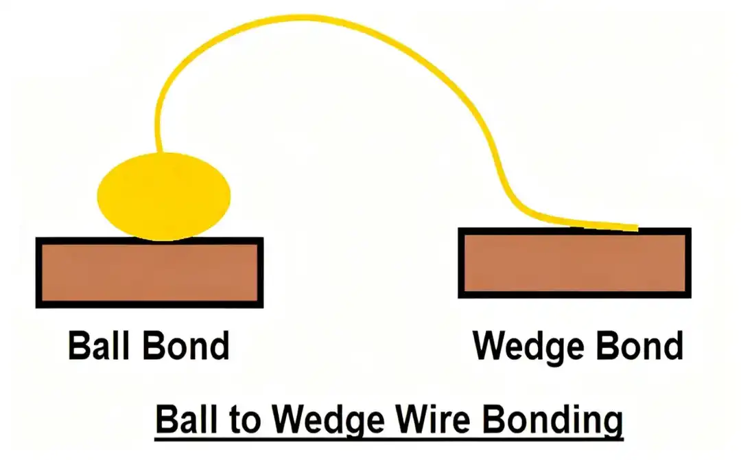
The most common wire bonding process is ball bonding, particularly in gold and copper wire bonding applications. It involves the creation of a sphere free air ball at the wire end, which is then pressed onto the bond pad by application of heat, ultrasonic energy, and pressure in the thermosonic process.
The use of gold wire bonding with ball bonds is not new, as gold is a very good conductor with high corrosion resistance. Copper bonding wire is gaining in popularity as a cheaper and more high-performance alternative, especially with power devices. Ball bonds are high-speed and non-directional, making them suitable for high-speed consumer electronics IC wire bonding.
Wedge bonding uses a wedge-shaped tool to press the bonding wire directly against the pad. This technique is widely used with aluminum wires in applications such as semiconductor wire bonding for automotive power devices and aerospace systems.
It provides fine-pitch capability, achieving dimensions as small as 15–25 μm. It is common in PCB wire bonding for direct chip-on-board assembly. Aluminum wedge bonds are cost-effective but are limited by pad spacing requirements.
Thermocompression bonding uses only heat and pressure and is slower but provides high reliability. In contrast, ribbon bonding uses flat ribbons instead of round wires for high-current or RF applications. Meanwhile, reverse bonding places a stud on the pad before bonding the wire to it. Finally, laser-assisted and photonic bonding represent advanced methods for MEMS, LEDs, and photonic devices.
The choice of bonding wire depends on conductivity, mechanical strength, cost, and reliability requirements.
Common bond wire materials include:
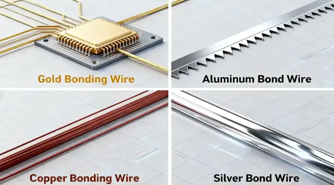
This is the most traditional material for gold bonding and IC wire bonding, providing excellent corrosion resistance and conductivity. It remains widely used in semiconductor wire bonding for critical applications.
Used primarily in wedge bonding, it is cost-effective and lightweight, making it ideal for power modules and PCB wire bonding.
Gaining dominance as a lower-cost alternative to gold, offering superior electrical and thermal conductivity. However, it requires protective coatings, such as Pd-coated copper bonding wire, to prevent oxidation.
Although less common, it offers the highest conductivity. Silver bond wire is suitable for niche applications requiring low-resistance bonded wires.
Pd-coated copper bonding wire combines copper's conductivity with palladium's oxidation resistance. Bimetallic and alloyed bond wires improve strength and thermal stability. These variations are vital for high-temperature and high-frequency semiconductor wire bonding.
Thin wires such as 17–25 μm are incorporated in fine-pitch IC wire bonding, while thicker wires from 100–300 μm, with ribbons used for even higher current applications. Loop height, heel angle, and bond wire geometry significantly influence quality.
To execute precise wire bonding processes, specialized equipment is essential:
• Wire bonders: Fully automatic, semi-automatic, and manual machines
• Capillaries: Suitable for gold wire bonding
• Wedge tools: Effective for aluminum and copper wire bonding
Modern machines provide precise control of ultrasonic force, temperature, and bonding time, which is decisive for miniaturized semiconductor wire bonding.
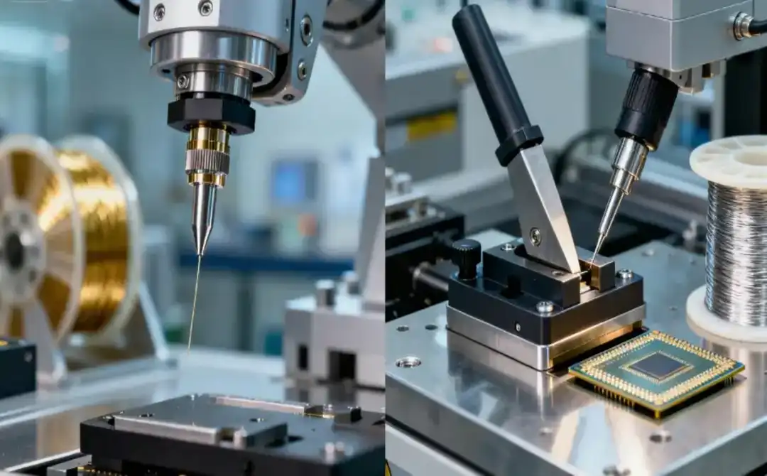
The wire bonding process consists of several sequential steps designed to create secure, conductive, and mechanically stable interconnects. These steps are common across most semiconductor wire bonding applications:
First, the semiconductor die is attached to a package substrate or PCB using adhesives, solder, or epoxy.
The choice of bonding wire—whether gold wire bonding, copper bonding wire, or aluminum—depends on cost, electrical, and thermal requirements.
Specialized capillaries and wedge tools guide the wire during the bonding cycle.
In gold bonding, the wire tip is formed into a free-air ball using electric flame-off (EFO), then bonded onto the pad with ultrasonic vibration and heat. In wedge bonding, the wire is pushed directly to form a wedge bond.
The wire is extended to the second connection point, forming an arch-shaped loop. The geometry of the bonded wire loop directly influences electrical performance quality.
The second end of the bond wire is welded to the target substrate and package pad.
This involves three tests:
• Pull tests
• Shear tests
• Visual inspections
These three tests ensure the wire bonding process follows industry standards such as MIL-STD-883.
The precision of each step determines yield, particularly for high-density IC wire bonding and PCB wire bonding, where pad size is as small as 40 micrometers with pitches under 70 μm.
Time is money in your projects – and PCBasic gets it. PCBasic is a PCB assembly company that delivers fast, flawless results every time. Our comprehensive PCB assembly services include expert engineering support at every step, ensuring top quality in every board. As a leading PCB assembly manufacturer, we provide a one-stop solution that streamlines your supply chain. Partner with our advanced PCB prototype factory for quick turnarounds and superior results you can trust.
Wire bonding applications are wide in different industries:
IC wire bonding is important in consumer electronics, including smartphones, laptops, and wearables. Copper wire bonding is also commonly used in automotive electronics such as power modules, sensors, and ECUs.
Also, bonding wires are needed in aerospace and defense applications, such as radar, satellites, and military electronics, which are of high quality. Additionally, medical devices such as pacemakers, hearing aids, and implants require the accuracy of semiconductor wire bonding.
In addition, optoelectronics and LEDs make use of PCB wire bonding, needed in chip-on-board LED arrays and CMOS image sensors.
Lastly, power electronics using SiC and GaN devices are also highly power-dependent on the use of thick copper bonding wire to enable efficient power management.
The issue of the quality of bonded wires is still a challenge despite progress in this area. These are bond failures, which are characterized by bond lift-off, heel cracks, and breakages during thermal cycling.
Also, problems of the material are caused by Au-Al intermetallic compounds (IMCs), copper oxidation, and silver tarnishing. Furthermore, geometrical stresses are evident when heel stress and crack propagation are exacerbated by the improper design of bond wire loops.
The compelling criteria used to select bonding wire materials and mechanisms are cost:
Gold wire bonding is also dependable and costly. Copper wire bonding offers significant reductions in the mass production of IC wire bonding. Aluminum bonding wire is a low-cost power electronics and PCB wire bonding.
There is a range of machine investments: semi-automatic bonders are tens of thousands of dollars, and fully automated machines are hundreds of thousands of dollars.
Wire bonding is one of the technologies that has been indispensable since 1960. The wire bonding process is very important in gold bonding, copper wire bonding, and PCB wire bonding.
Although flip-chip and modern interconnects have emerged, bonding wires will still be at the center of semiconductor wire bonding. Wire bonding will be able to fulfill the requirements of the next generation of electronics with the current advancement in materials, automation, and design.

Assembly Enquiry
Instant Quote
Phone contact

+86-755-27218592
In addition, we've prepared a Help Center. We recommend checking it before reaching out, as your question and its answer may already be clearly explained there.
Wechat Support

In addition, we've prepared a Help Center. We recommend checking it before reaching out, as your question and its answer may already be clearly explained there.
WhatsApp Support

In addition, we've prepared a Help Center. We recommend checking it before reaching out, as your question and its answer may already be clearly explained there.