Today's electronic devices, which range from simple smartphones to advanced medical technology, are all heavily reliant on powerful integrated circuits (ICs), but also on the chip package types that allow these ICs to function reliably in real-world conditions. The packaging provides the necessary protection for fragile silicon, provides electrical connections to the printed circuit board (PCB), and controls how dense or robust the final design can be.
Perhaps the most accepted and widely adopted group of package types from the modern ages of electronics is the small outline family of packages, which includes SOP, SSOP, TSSOP, and TSOP package types. Each of these family members was designed to meet specifications for reducing size, increasing density, and lowering cost (often in that sequence). The SSOP, Shrink Small Outline Package was designed as a compromise in the evolution between design confines of size and manufacturability of the package process.
This article will take an informed look at the SSOP package full form and features compared to its closely related family in the SOP family. We will review the SSOP package in the dimensions of PCB and PCBA production in an understanding of why the use of SSOP still exists despite the advancement of its various package technologies.

What is SSOP Package?
The full form of SSOP is Shrink Small Outline Package. It is a condensed form of the typical SOP (Small Outline Package). When electronics began to shrink quickly in the 1980s and 1990s, SSOP was introduced before the widespread adoption of CSP and BGA, offering engineers a simpler way to reduce board footprint.
Structurally, the SSOP package features a rectangular molded plastic body with gull-wing leads extending from the sides. These leads have a finer pitch compared with SOP, typically 0.65 mm and sometimes as fine as 0.5 mm. This tighter spacing allows for higher pin counts in smaller packages, supporting compact and efficient PCB layouts.
In the broader context of chip package types, the development can be seen as:
DIP package – Dual In-line Package, the old through-hole classic. Very easy to solder but uses lots of board space.
SOP – Small Outline Package, the surface-mount replacement for DIP, allowing for moderate size minimization.
SSOP – Shrink Small Outline Package, shrinking the body size and the pin pitch for increased density.
TSSOP – Thin Shrink Small Outline Package, shrinking the package height even further.
TSOP – Thin Small Outline Package, designed for memory ICs with very thin profiles.
Thus, SSOP represents a transitional yet highly practical choice in the push toward miniaturization.
Key Features of SSOP IC Package

The SSOP IC package comes with several distinct features that explain its long-standing popularity.
1. Reduced Lead Pitch
In comparison, SOP normally uses a 1.27 mm pitch, and SSOP reduces it even more to under 0.65 mm. In the narrowed pitch, more leads can fit into a small package width, and circuit density is therefore increased.
2. Smaller Footprint
By decreasing the overall dimensions of the body, the SSOP package optimizes the utilization of PCB real estate. In scenarios where every square millimeter is of significance, this reduction becomes essential.
3. Higher Circuit Density
With more pins packed into smaller space, SSOP accommodates increasingly sophisticated IC functions with minimal increase in board size. This is critically necessary for consumer electronics, where high-feature product devices need to stay small.
4. Balanced Electrical and Thermal Properties
Even though SSOP does not rival the superior performance of the latest-generation packages like QFP or BGA in heat dissipation, it maintains the reliable electrical parameters for medium-power applications. In addition, it achieves a practical balance among dimensions and stability.
5. Cost-Effective Production
As SSOP is an extension of tried-and-tested surface-mount manufacturing methods, it is still cost-effective compared to more recent and sophisticated packaging formats.
Overall, the SSOP package provides the best combination of benefits: it is more compact than the SOP, cheaper to produce than ultra-fine-pitch versions, and is widely supported by all industries.

SOP, SSOP, TSSOP and TSOP
To fully understand SSOP, we must look at its place within the broader SOP family. Each variant was designed to address evolving needs in electronics design.

SOP (Small Outline Package)
SOP was developed as a surface-mount version of the DIP package. SOP packages, with their usual 1.27 mm lead pitch and body thickness of roughly 1.5–2.0 mm, presented lower board usage than the DIP but were still hardy and rugged and easy enough to handle. They became very commonplace for logic ICs, operational amplifiers, and numerous general-purpose devices.
SOP's strengths are simplicity and reliability. However, as devices shrank, their relatively large footprint became a limitation.
SSOP (Shrink Small Outline Package)
The SSOP package improved upon the SOP package by decreasing the lead pitch to 0.65–0.8 mm and by decreasing the body width to lessen the footprint. Unquestionably, plenty of options including layouts with 16–48 pins! SSOP was well-suited for microcontrollers, signal processor packages, and consumer electronics successfully.
The SSOP package served as a transitional format between older SOP designs and newer, thinner package types. The SSOP fills the density needs and manufacturability. That is precisely why SSOP packages are still so well-used, since they were developed.
TSSOP (Thin Shrink Small Outline Package)
When phones, tablets, and portable electronics needed thinner boards, the TSSOP package made its appearance. It was only 0.8–1.2 mm thick and reduced the height by quite a bit compared to SOP and SSOP. The lead pitch could be down to just 0.5 mm and up to 64 pins were accommodated without consuming too much vertical height.
TSSOP proved invaluable within small size applications where a small volume is as important as the footprint, for example, handheld medical applications and communication integrated circuits.
TSOP (Thin Small Outline Package)
Eventually, the TSOP met the unique needs of the memory market. Through the use of a long, flat layout under 1.2 mm thickness and 0.5 through 0.8 mm pitches, the TSOP could accommodate very high pin counts, sometimes over 128 pins. This layout is especially ideal for DRAM, Flash memory, and solid-state storage devices that require stacking and compact arrays.
SOIC vs SSOP Package
When comparing chip package types, engineers often pit the SOIC vs SSOP package because both exist in great abundance within the medium-pin-count IC arena. Although both are members of the surface-mount clan, they are designed for differing priorities.

The SOIC (Small Outline Integrated Circuit) package is one where the size is relatively large, with the usual lead pitch equating to 1.27 mm. This characteristic aids assembly handling, improves soldering misalignment tolerance, and makes the package especially desirable for high-speed automated production facilities where density is of lesser importance. In addition, SOIC packages normally equate to a higher body thickness, thus adding increased mechanical strength and qualifying them for industrial or higher reliability applications.
As an alternative, the SSOP package decreases the pitch to 0.65 mm or 0.8 mm, therefore cutting the width roughly in half compared to the equivalent-pin-count SOIC package. This minimization facilitates higher circuit density and conserves PCB board space, an absolute necessity for small size consumer applications such as cameras, cell phones, or portable medical devices. The higher pitch, however, results in more stringent soldering process requirements and also increases the risk of solder bridging during the reflow step.
In PCB assembly, SOIC is easier and cheaper to install, but SSOP calls for very accurate stencil layout, positioning, and inspection. Nevertheless, from a design efficiency perspective, SSOP offers clear benefits where PCB space is at a premium.
In short, the choice between SOIC vs SSOP package is a classic trade-off:
SOIC = simplicity, robustness, and ease of manufacturing.
SSOP = miniaturization, density, and space savings.
This is why SOIC still dominates in industrial electronics and legacy systems, while SSOP has become the preferred option for compact, modern consumer products.
Applications of SSOP Package
Because of its versatility, the SSOP IC package is found in a wide range of industries.
1. Consumer Electronics – Laptops, cameras, game consoles, and smartphones use SSOP technology-based ICs for signal processing, power control, and system management.
2. Automotive Systems –Engine control units (ECUs), infotainment systems, and sensors for vehicles apply SSOP integrated circuits (ICs) due to their compact size and stable performance.

3. Industrial Electronics – For factory automation and programmable controllers, SSOP provides reliable, high-density circuit configurations.
4. Medical Devices –Small form factor diagnostic tools and portable monitors benefit from the SSOP's balance of dimensions and manufacturability.
Across all these fields, the SSOP package allows designers to maximize functionality without overly complicating assembly.
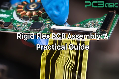
PCB and PCBA Considerations for SSOP

Integrating SSOP devices into a PCB requires careful design.
PCB Footprint Design –Pads need to be very carefully sized to JEDEC specifications. The designer needs to trade solder mask clearance for solder bridging among thin leads.
Reflow Soldering –Alignment is critical with lead pitches as small as 0.65 mm. Accurate solder paste printing and reflow profiles are necessary for the avoidance of defects.
Inspection and Testing – Automated Optical Inspection (AOI) is similarly widely employed for lead integrity testing since it is not feasible for human inspection at such small volumes.
Reliability – While robust, SSOP devices may face issues such as solder bridging or misalignment in mass production. Proper PCBA processes minimize these risks.
So, while SSOP is high-density and provides a physical size advantage, SSOP packaging requires more constraints around PCB assembly than older chip package types like SOP or DIP. Even though SSOP devices are very robust, they can still experience solder bridging or misaligned pads in a production scenario. Effective PCBA processes mitigate these risks. So, while SSOP provides a relatively high-density option, it does so at a higher precision requirement than older chip package types like SOP or DIP.
Conclusion
The SSOP package is a significant milestone for the evolution of integrated circuit packaging. Its full form, Shrink Small Outline Package, accurately describes its mission: higher density within the reduced footprint with manufacturability preserved.
When one considers SOP and SSOP package, the decision more often than not is one of space efficiency or ease of assembly. SOP is easier but bigger; SSOP minimizes size at the expense of more precise manipulation. Compared to relatives TSSOP and TSOP, SSOP is still the compromise: more slender and more compact than SOP, but more specialized than TSOP or more ultrathin than TSSOP. Although higher-end solutions such as BGA and CSP reign supreme among high-end units, the SSOP is still very prolific. Its combination of reliability, cost, and density makes it an attractive package for the vast majority of consumer, auto, and commercial applications.
As electronic devices become increasingly advanced, packaging strategies for the future will emphasize miniaturization, greener materials, and better thermal designs. Yet the SSOP IC package will likely remain relevant, proving that sometimes the best solutions are those that strike the right balance between innovation and practicality.
 About PCBasic
Time is money in your projects – and PCBasic gets it. PCBasic is a PCB assembly company that delivers fast, flawless results every time. Our comprehensive PCB assembly services include expert engineering support at every step, ensuring top quality in every board. As a leading PCB assembly manufacturer, we provide a one-stop solution that streamlines your supply chain. Partner with our advanced PCB prototype factory for quick turnarounds and superior results you can trust.