Global high-mix volume high-speed PCBA manufacturer
9:00 -18:00, Mon. - Fri. (GMT+8)
9:00 -12:00, Sat. (GMT+8)
(Except Chinese public holidays)
Global high-mix volume high-speed PCBA manufacturer
9:00 -18:00, Mon. - Fri. (GMT+8)
9:00 -12:00, Sat. (GMT+8)
(Except Chinese public holidays)
HomePage > Blog > Knowledge Base > PCB Edge Plating: A Complete Guide
As electronic products continue to evolve towards high-frequency operation, high-density integration and miniaturized structures, the design and manufacturing pressure that PCBs bear in practical applications is also increasing. This may bring about a series of problems, including affected signal integrity, more difficult control of electromagnetic interference (EMI), or unstable grounding reliability. In many practical cases, these problems do not originate from the circuit design itself, but are concentrated in the PCB edges, an area that is often underestimated.
In RF, industrial control, automotive electronics, and products with high reliability requirements, a common and mature solution is PCB edge plating. By extending the PCB copper plating from the top layer all the way to the bottom layer and covering the sides of the circuit board, edge plating can make the outline of the PCB no longer just a cut edge, but a part with conductive and structural support capabilities.
Although in some projects, PCB edge plating is often regarded as an optional process, it has effects on EMI control, grounding continuity, mechanical edge reinforcement and assembly reliability. This article will focus on PCB edge plating, systematically sorting out the value of this process in practical engineering from several aspects such as PCB edge plating design, manufacturing, application, limitation and detection, to help you determine whether it is suitable for your product.

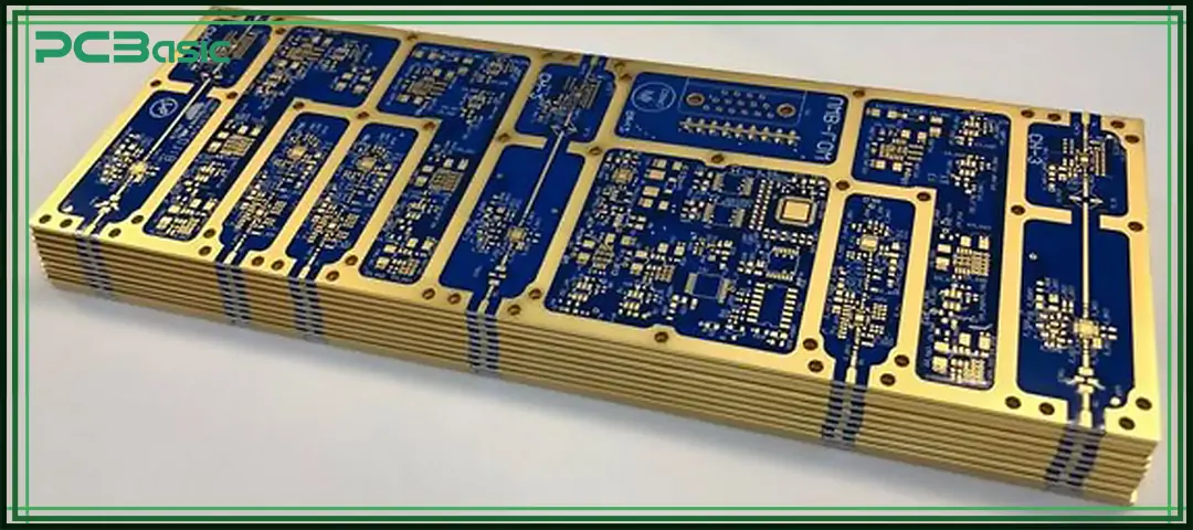
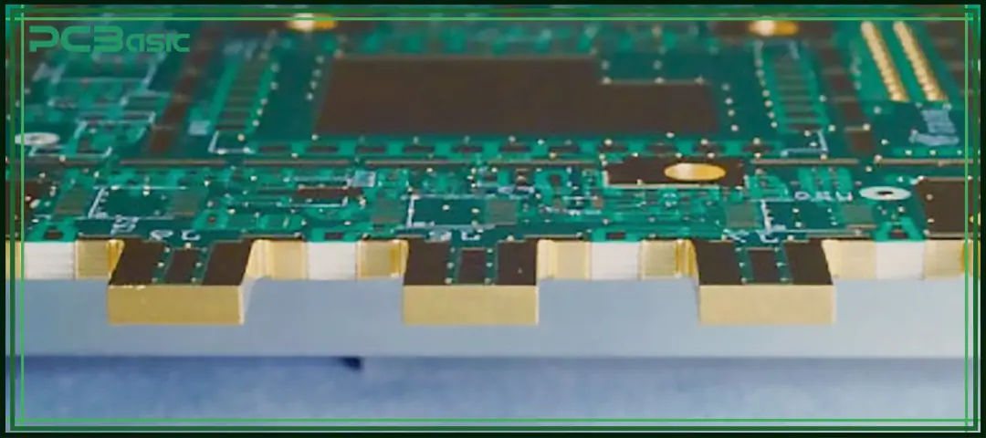
PCB edge plating, also known as side plating or edge metallization, is a rather special PCB copper plating process. In simple terms, after the shape of the circuit board is formed, copper plating is applied to the sidewall of the PCB, allowing the copper layer to connect from the top layer to the bottom layer and form a continuous metal layer along one or more edges of the circuit board.
Unlike a conventional copper pour, which is only laid inside the board and ends at the outline, edge plating intentionally wraps the copper layer to the outside of the PCB, causing the PCB copper plating to cover the sidewalls of the circuit board. In this way, the PCB edge is no longer just a cut boundary, but becomes a part that has the ability to conduct electricity and also enhances the mechanical strength.
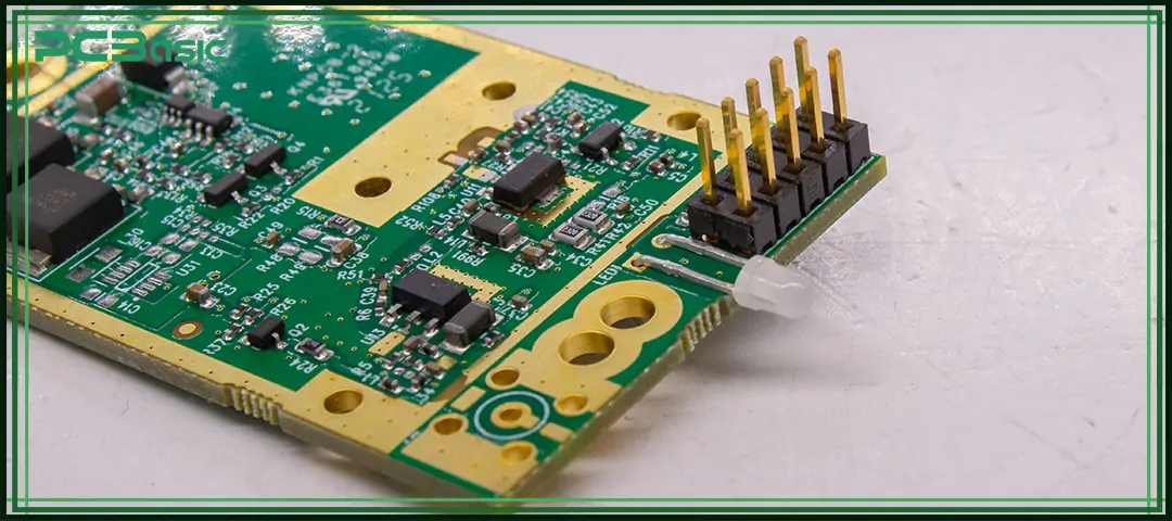
In the PCB edge plating process, common surface finishes include ENIG, ENEPIG, HASL or immersion silver, as long as electrical continuity is maintained. Under suitable process conditions, PCB edge plating can not only be applied to the outer contour edges of circuit boards, but also to some internal slots or cutout areas to achieve specific functions such as grounding, shielding or structural connections.
Not every PCB needs to use PCB edge plating. However, in some projects with high requirements for performance and reliability, it is often difficult to completely solve the problem by relying on conventional routing or structural design alone. In such a case, edge plating is considered.
Generally speaking, when the following requirements arise in the design, engineers will give priority to using edge copper plating:
• Improve electrical grounding and current flow
• Enhance EMI / EMC performance
• Strengthen PCB edges against mechanical stress
• Enable edge soldering or edge-based interconnections
• Improve contact with metal enclosures or shielding structures
The following are some common reasons for using PCB edge plating:
One direct function of PCB edge plating is to form a continuous conductive path on the outer perimeter of the PCB. The PCB copper plating formed along the edge of the board can make the return current flow more smoothly and the impedance more stable, thereby reducing signal fluctuations and noise problems. For multilayer boards, PCB edge plating can also connect each ground layer together, reducing interference between layers.
When the PCB edge plating is connected to ground, it effectively forms a metallic barrier around the PCB. This can effectively reduce the leakage of electromagnetic radiation from the board edges and also lower the possibility of external interference entering the circuit.
The edges of a PCB are most prone to experience mechanical stress during assembly, handling and operation. PCB edge plating adds a layer of metal to the board edge, which is equivalent to adding a protective layer to the PCB, reducing the risk of chipping, cracking or delamination. For PCBs that need to be inserted into metal casings or rails, this structure can also enhance wear resistance and maintain stable electrical contact.
PCB edge plating enables the board edge itself to be used for soldering and electrical connections. Whether it is edge soldering, PCB-to-PCB interconnection, or grounding with a metal casing, extending PCB edge plating to the edge of the board can make the structure simpler, the connection more reliable, and at the same time reduce the reliance on connectors.

Due to the comprehensive advantages of PCB edge plating in electrical performance, mechanical strength and EMC performance, this process is widely used in multiple industries and application scenarios, including:
• RF and wireless modules (Wi-Fi, Bluetooth, GNSS)
• Multilayer high-speed digital PCBs
• Small form factor and module-based designs
• PCBs installed in metal enclosures or shielded housings
• Industrial control and automation electronics
• Automotive electronic systems

Time is money in your projects – and PCBasic gets it. PCBasic is a PCB assembly company that delivers fast, flawless results every time. Our comprehensive PCB assembly services include expert engineering support at every step, ensuring top quality in every board. As a leading PCB assembly manufacturer, we provide a one-stop solution that streamlines your supply chain. Partner with our advanced PCB prototype factory for quick turnarounds and superior results you can trust.
Compared with the standard PCB plating process, PCB edge plating has higher requirements for processing accuracy and process stability. In addition to the conventional copper plating on the hole walls and circuits, it is also necessary to form a reliable and continuous copper layer on the sides of the PCB.
Generally speaking, the manufacturing process of copper plating on PCB edges mainly includes the following key steps:
Before edge plating is applied, the PCB must first be routed to its final outline. The flatness and surface quality of the board edge directly affect the adhesion of the subsequent copper plating.
The PCB edges are cleaned and activated to ensure that the copper layer can firmly bond to the base material.
Through electroplating, copper is extended from the top layer to the bottom layer and deposited onto the sidewalls of the PCB, forming a complete edge plating (edge plating) structure.
Edge plating is typically performed within the same process flow as through-hole plating to ensure consistency and reliability between sidewall plating and via wall plating.
Depending on application requirements, surface finishes such as ENIG, ENEPIG, HASL, or immersion silver are applied to the plated areas.
In the entire process, edge preparation is a key factor that affects the quality. If burrs or uneven edges occur during the shape processing, it may cause discontinuity of the through-hole wall plating and also shorten the adhesion life of edge plating. Therefore, PCB edge plating has high requirements for the routing accuracy, machining parameters, and overall process stability.

Reasonable design is the key to ensuring the manufacturability and reliability of PCB edge plating.
The main design rules include:
|
Design Item |
Requirement |
Purpose / Notes |
|
Definition of plated edge area |
Use overlapping copper to define the areas requiring edge plating |
Ensures continuous and reliable PCB edge plating during fabrication |
|
Copper overlap width |
Copper overlap with the board outline should be ≥ 0.5 mm |
Insufficient overlap may result in incomplete plating or poor adhesion |
|
Connection layers |
Layers connected to the plated edge must provide sufficient copper width or copper pour |
Ensures reliable electrical connection to PCB copper plating |
|
Non-connection layers |
Copper on non-connected layers must maintain adequate clearance from the board edge |
Prevents short circuits during the PCB plating process |
|
Internal power planes |
Do not route power planes directly to the PCB edge |
Avoids short-circuit risks during edge plating |
|
Edge-mounted connectors |
For edge-mounted connectors (e.g., SMA), use polygon cutouts |
Prevents unintended shorts between pads and edge plating |
|
Internal slots / cutouts |
Clearly define plated or non-plated slot edges in design files |
Avoids manufacturing ambiguity and DFM issues |
|
Fabrication documentation |
Clearly specify plated edges in fabrication drawings and order notes |
Reduces back-and-forth communication and production delays |
Inspection is a key stage to ensure the reliability of PCB edge plating.
The main inspection points include:
|
No. |
Inspection Category |
Key Check Point |
Acceptance Criteria / Control Focus |
|
1 |
Process documentation & manufacturability |
Gerber files and fabrication drawings clearly specify plated edges |
Plated edge locations are clearly defined with no ambiguity |
|
2 |
Panelization & process structure |
Routing tabs / non-plated areas are properly reserved |
Panel support does not interfere with edge plating continuity |
|
3 |
Edge plateability |
PCB edges are flat, smooth, and free of burrs or delamination |
Edges are suitable for edge plating |
|
4 |
Edge surface preparation |
Cleaning and activation of board edges |
No oil, oxidation, or residue present |
|
5 |
Sidewall copper continuity |
Edge plating coverage along PCB sidewalls |
Continuous plating, no exposed base material |
|
6 |
Plating integrity & adhesion |
Copper layer condition |
No peeling, cracking, or flaking allowed |
|
7 |
Via-to-edge consistency |
Continuity between via wall plating and edge plating |
Smooth transition, no discontinuity |
|
8 |
Non-plated area control |
Routing tab / keep-out regions |
No unintended copper plating |
|
9 |
Surface finish condition |
ENIG / HASL / Immersion Silver quality |
Uniform coverage, no oxidation or contamination |
|
10 |
Electrical continuity & grounding |
Conductivity and grounding of plated edges |
Stable continuity, resistance within design limits |
|
11 |
EMC-related grounding |
Edge plating grounding per design intent |
No floating or unintended isolation |
|
12 |
Visual consistency |
Color, width, and boundary of plated edges |
Uniform appearance, clean boundaries |
|
13 |
Packaging & transport protection |
Edge protection during packing and shipment |
No edge damage after transportation |
PCB edge plating is not merely an optimization of appearance. If implemented properly during the design and manufacturing phases, it can bring about very significant improvements in electrical performance, EMI control, mechanical reliability, and assembly stability.
By extending the PCB copper plating to the edge of the circuit board, edge plating can achieve more stable grounding, more effective electromagnetic shielding, stronger board edge structure, and reliable interconnection methods that are difficult to achieve in traditional PCB design.
Of course, to truly bring out the value of PCB edge plating, the prerequisite is to do a good job in design planning, strictly follow manufacturing rules, maintain clear and accurate process communication with manufacturers, and cooperate with sufficient testing and verification. A comprehensive understanding of the PCB plating process and its limitations in terms of cost and technology is the key to making correct engineering decisions.
In appropriate application scenarios, PCB edge plating remains one of the most effective and mature technical solutions for high-performance and high-reliability electronic products at present.

Assembly Enquiry
Instant Quote
Phone contact

+86-755-27218592
In addition, we've prepared a Help Center. We recommend checking it before reaching out, as your question and its answer may already be clearly explained there.
Wechat Support

In addition, we've prepared a Help Center. We recommend checking it before reaching out, as your question and its answer may already be clearly explained there.
WhatsApp Support

In addition, we've prepared a Help Center. We recommend checking it before reaching out, as your question and its answer may already be clearly explained there.