Global high-mix volume high-speed PCBA manufacturer
9:00 -18:00, Mon. - Fri. (GMT+8)
9:00 -12:00, Sat. (GMT+8)
(Except Chinese public holidays)
Global high-mix volume high-speed PCBA manufacturer
9:00 -18:00, Mon. - Fri. (GMT+8)
9:00 -12:00, Sat. (GMT+8)
(Except Chinese public holidays)
HomePage > Blog > Knowledge Base > PCB Solder Mask: Materials, Thickness, Design & Process
When you first come into contact with PCB design or manufacturing, you will learn about the solder mask. The study of the PCB solder mask is an indispensable aspect in the manufacturing of circuit boards. The solder mask is not only for coloring the PCB, but more importantly, it also provides protection for the circuit board. In today's article, we will introduce to you:
What is the PCB solder mask
Why can't PCB do without it
Solder mask materials and types
Solder mask colors
PCB solder mask DFM guidelines
Manufacturing process of solder mask
First, let's introduce what a PCB solder mask is.
The PCB solder mask is also known as the soldermask or solder resist layer. It is a protective coating that covers the surface of the copper wires on the PCB. This layer of protective coating can isolate the air (moisture, dust, and contaminants, etc.) and solder, preventing the copper foil from oxidizing. In addition, during the soldering process, it can also avoid solder bridges, thereby maintaining the reliability and cleanliness of the circuit board. As shown in the following picture, this is the PCB solder mask layer.
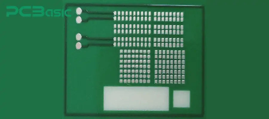
The solder mask on most circuit boards we see is green, but its color is not limited to green. It can also be black, white, red, blue, and other different colors.
The solder mask layer is crucial in PCBs and has the following aspects of significance:
Preventing short circuits: The solder mask layer can prevent adjacent pads from shorting each other, preventing solder from flowing to unintended connection areas during the soldering process.
Protecting the copper surface from oxidation or corrosion
Improving insulation: The solder mask layer forms an insulating layer between different copper wires, reducing leakage or signal interference.
Facilitating automated soldering: The solder mask layer can limit the spread of solder, and when combined with solder paste printing, it enhances the efficiency of automated soldering.
Helping in component placement: After the solder mask layer is opened, only the pads are exposed, clearly distinguishing the solderable areas.
The selection of appropriate solder mask materials is also very important for PCB manufacturing. The ink used for the soldering layer of the PCB is a composite material consisting of resin, curing agent, pigment and additives. Among them, the resin is the main component. It determines the adhesion, hardness and high-temperature resistance of the soldering layer on the PCB. Common types of resins include epoxy resin, photoimageable polymer, and UV-Curable.
In addition, the curing agent is used to form the film of the ink. The pigment determines the color of the soldering (such as green, black, white). Fillers and additives are used to enhance thickness, scratch resistance and leveling effect. For photosensitive solder mask ink, a photoinitiator is added to enable ultraviolet exposure and development capabilities.
Next, I will introduce to you four widely used types of solder mask.
1. Epoxy Liquid Solder Mask
Epoxy liquid solder mask was one of the earliest types of solder mask materials used. The ink is printed onto the surface of the PCB through screen printing, and then baked for curing.
Features:
Low cost, simple process
Suitable for ordinary PCB production
Limited resolution, not suitable for fine-pitch pads
Uneven thickness
General chemical resistance and heat resistance
This solder mask layer is commonly used in low-end consumer electronics, remote controls, power boards, and simple single-sided/double-sided PCBs.
2. LPI Solder Mask
Features:
High precision, uniform thickness
Suitable for fine pitch, BGA, QFN and high-density wiring boards
Good adhesion, strong electrical insulation
Resistant to chemical corrosion and high temperature
Suitable for automation and mass production
It is often used in mobile phone mainboards, automotive electronics, industrial control, medical equipment, 5G communication boards, etc.
3. Dry Film Solder Mask
Features:
High resolution, clear pad edges
Good consistency of solder mask thickness
Suitable for high-density and high-precision wiring
Complex process, high cost
High requirements for board surface flatness, poor flexibility
4. UV-Curable Solder Mask
Features:
Fast curing speed, high efficiency
Low volatile organic compounds, more environmentally friendly
Less hardness and heat resistance compared to LPI or dry films
Lower long-term reliability
Not suitable for high-temperature soldering or harsh environments
The previous section introduced the materials and types of the PCB solder mask layer. Now, in this part, we will discuss the thickness of the solder mask layer.
The thickness of the solder mask layer directly affects the soldering quality, insulation performance, solder mask strength, and the reliability of the PCB. Its thickness is not only determined by the material type and coating method, but also related to factors such as whether there are windows and the copper surface structure. Typical solder mask thickness includes:
|
PCB Area |
Standard Thickness |
Notes |
|
Copper trace surface |
10–30 μm |
Most commonly used thickness range |
|
Pad area |
≈ 0 μm |
Pads are fully opened, no solder mask remains |
|
Large copper planes |
30–50 μm |
Thicker coating for better oxidation protection and insulation |
|
Solder mask dam (solder mask bridge) |
Width ≥ 0.10 mm |
Thickness is the same as the overall solder mask layer, not calculated separately |
|
Solder mask expansion |
0.05–0.10 mm |
Clearance between pad edge and solder mask opening to compensate for alignment tolerance |
The solder mask thickness determines the coverage effect, while the solder mask expansion determines whether the pads can be smoothly exposed and completed with soldering. We have already introduced the relevant content about PCB solder mask thickness before. Now, let's briefly introduce the design aspects related to solder mask expansion. (Learn more about solder mask expansion here!)
|
Parameter |
Recommended Value |
Explanation |
|
Mask opening larger than pad |
+0.05 to +0.10 mm |
Known as solder mask expansion, prevents mask from encroaching onto pads due to alignment errors. |
|
Minimum solder mask dam width |
≥ 0.10 mm (4 mil) |
Ensures proper mask stability; smaller than this may cause breaks or solder bridging. |
|
BGA pad solder mask design |
Full opening or tenting based on pitch |
For fine-pitch BGA, solder mask between pads may be removed to avoid manufacturing defects. |
From the above content, we can understand that by controlling the solder mask thickness to be within 10–30 μm (in the circuit area), and keeping the solder pad area bare or in a very thin state, while ensuring a 0.05–0.1 mm solder mask window expansion in the design, the best soldering and protection effect can be achieved.
Green solder mask is the most commonly used color in PCB manufacturing. This is because green is easy to obtain stable line boundaries during exposure and development processes. Additionally, quality inspectors can more easily identify defects such as solder residue, solder bridges, and scratches on green circuit boards. However, the solder mask layer is not limited to green. As product appearance requirements, functional needs, and brand recognition increase, PCB manufacturers also offer a variety of solder mask colors for selection:
|
Solder Mask Color |
Characteristics |
Common Applications |
|
Green solder mask |
Clear imaging, high heat resistance, best contrast for inspection |
Industrial control boards, communication devices, most standard PCBs |
|
Black solder mask |
Sleek appearance but makes solder joint inspection difficult; absorbs heat |
Audio equipment, high-end electronics, appearance-focused PCBA |
|
White solder mask |
Strong light reflection, ideal for LED PCBs; but easily stained |
LED lighting boards, home appliance PCBs, smart home control boards |
|
Red / Blue / Yellow solder mask |
Bright color, easy for functional differentiation or visual display |
Development boards, demo/display boards, custom-brand PCBs |
|
Matte solder mask |
Non-reflective, premium texture, but higher manufacturing difficulty |
Gaming devices, consumer electronics, branded PCBA |
Does the color of solder mask affect the performance of the circuit board? The color of solder mask itself does not change the conductive or insulating performance of the PCB. However, it does have some impacts during manufacturing and inspection:
①Different colors have an effect on the solder mask process of the PCB. Dark-colored inks, such as black solder mask, absorb heat quickly, while white solder mask reflects light strongly.
②The color of solder mask affects the quality of identifying solder points during inspection.
③ It influences the appearance and brand recognition.
In the following section, we will present several suggestions regarding the PCB solder mask DFM:
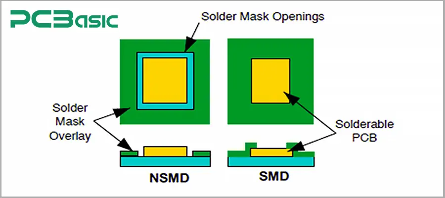
1. The solder mask expansion must be properly controlled. The solder mask expansion refers to the distance between the pad size and the solder mask opening. The recommended expansion value for solder mask is 0.05–0.10 mm.
If the expansion is too small, the solder mask ink may cover the pad, affecting the solder wetting. If the expansion is too large, the exposed copper area around the pad increases, making it prone to oxidation.
Therefore, the solder mask expansion should be appropriate.
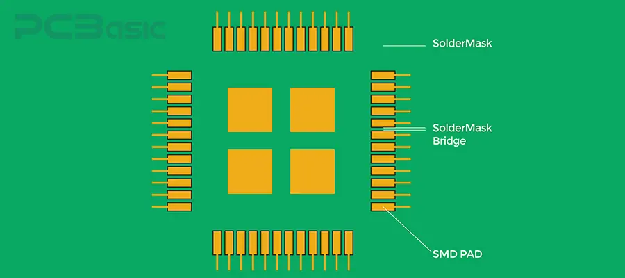
2. The width of the solder bridge must meet the minimum requirement. The solder bridge is a thin solder strip used for isolation between the pads. It is recommended that the minimum width be ≥ 0.10 mm.
3. For fine-pitch packaging such as BGA, it is necessary to avoid designing a solder mask between the pads. For BGA and devices with pad spacing less than 0.25 mm, either NSMD or SMD methods can be adopted. It is not recommended to place a solder mask layer between the pads; otherwise, it may cause poor soldering or solder ball short circuits.
4. Via-in-Pad must be filled or covered. If there is an overlap between pads and holes in the PCB design, the holes need to be filled, plugged, or tented.
5. The soldering area should avoid the positioning points and test points. The fiducial points used for positioning and the electrical test points should have their copper surfaces exposed and not be covered by the soldering mask; otherwise, it will affect the optical recognition or probe contact.
6. The alignment of the solder mask layer must be precise. If the solder mask layer is not aligned correctly with the circuit layer, it will result in:
The solder pads are partially covered or the opening positions are misaligned.
The local solder mask thickness is uneven.
During soldering, it is prone to cause solder bridges or oxidation of the solder pads.
The solder mask layer is also an indispensable step in PCB manufacturing. Below is the common process flow of PCB soldering.
1. Board surface cleaning and copper surface pretreatment
Before applying the solder mask ink, the PCB surface must be thoroughly cleaned. The oxide layer, oil stains, fingerprints, and dust on the circuit board need to be removed. Sometimes, a mild etching treatment is also performed to enhance the adhesion between the solder mask ink and the copper surface.
If the cleaning is not done properly, the subsequent solder mask layer process is likely to result in peeling, bubbles, or detachment.
2. Solder mask ink coating
After cleaning, the PCB needs to be coated with solder mask ink. This can be done through screen printing, spraying or curtain coating methods. On the copper lines, the thickness of the anti-soldering layer is generally controlled at 10–30 μm.
3. Pre-baking
After coating, the PCB will be placed in a drying oven for a low-temperature pre-baking process. This step is to slightly cure the surface of the solder mask ink, facilitating the subsequent exposure alignment, and preventing it from being sticky or flowing.
4. UV Exposure
This step determines whether the copper in the pad area is exposed. It is a crucial stage in forming the solder mask pattern. First, a film is applied to the PCB and aligned with the pads. Then, the solder mask ink in the non-pad areas is cured by ultraviolet light. After that, the areas not exposed at the pad positions remain in a state that can be developed.
5. Developing
After exposure, the PCB enters the developing tank. The unexposed solder mask ink is removed, and the pads are exposed. The exposed and cured parts remain on the board surface.
6. Complete Curing
After the development process is completed, the solder mask layer needs to be fully cured. Usually, it is baked at a temperature range of 140–160°C. UV solder mask ink is cured using ultraviolet light. This process ensures that the solder mask layer achieves the final hardness, chemical resistance, and insulation properties.
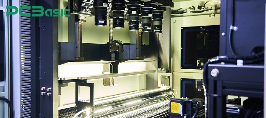
7. Inspection
Finally, the entire solder mask PCB layer is inspected. We need check:
Is the solder mask offset or pressing on the pads?
Is the pad expansion complete and is there no residual ink on the pads?
Is the solder mask thickness uniform?
There are no bubbles, no oil shedding, and no contamination.
The solder mask layer on a PCB is an important protective coating on the board. It comes in various colors such as green, black, white, yellow, and blue, among others. Although it is only a thin layer, it has a significant impact on soldering quality, electrical insulation, oxidation resistance, and the long-term reliability of the PCB. It is very necessary to learn about the relevant knowledge of the PCB solder mask layer.
 About PCBasic
Time is money in your projects – and PCBasic gets it. PCBasic is a PCB assembly company that delivers fast, flawless results every time. Our comprehensive PCB assembly services include expert engineering support at every step, ensuring top quality in every board. As a leading PCB assembly manufacturer, we provide a one-stop solution that streamlines your supply chain. Partner with our advanced PCB prototype factory for quick turnarounds and superior results you can trust.

Assembly Enquiry
Instant Quote
Phone contact

+86-755-27218592
In addition, we've prepared a Help Center. We recommend checking it before reaching out, as your question and its answer may already be clearly explained there.
Wechat Support

In addition, we've prepared a Help Center. We recommend checking it before reaching out, as your question and its answer may already be clearly explained there.
WhatsApp Support

In addition, we've prepared a Help Center. We recommend checking it before reaching out, as your question and its answer may already be clearly explained there.