Global high-mix volume high-speed PCBA manufacturer
9:00 -18:00, Mon. - Fri. (GMT+8)
9:00 -12:00, Sat. (GMT+8)
(Except Chinese public holidays)
Global high-mix volume high-speed PCBA manufacturer
9:00 -18:00, Mon. - Fri. (GMT+8)
9:00 -12:00, Sat. (GMT+8)
(Except Chinese public holidays)
HomePage > Blog > Knowledge Base > PCB Assembly Process: A Complete Step-by-Step
Modern electronic products - from smartphones and medical devices to industrial controllers and satellites - all rely on a key manufacturing stage: PCB assembly. Without precise component placement, reliable solder joints and strict testing procedures, even the most advanced circuit design can only remain at the "bare board" stage and cannot truly perform its intended function.
PCB assembly, also known as PCBA, serves as a crucial bridge between product design and actual functionality. Through precise equipment and standardized processes, the assembly of PCBs is completed, and ultimately, the manufactured circuit boards are transformed into stably operating electronic systems. In the current highly competitive market environment, high-quality printed circuit board assembly is not only related to the reliability of product performance, but also directly affects the large-scale production capacity and the overall cost control level.
This article will provide a systematic and step-by-step explanation of the PCB assembly process, introducing how electronic components are installed, soldered, inspected and validated. Meanwhile, the focus will also be on analyzing why PCB assembly and manufacturing occupy such a core position in the electronics manufacturing services (EMS) system.
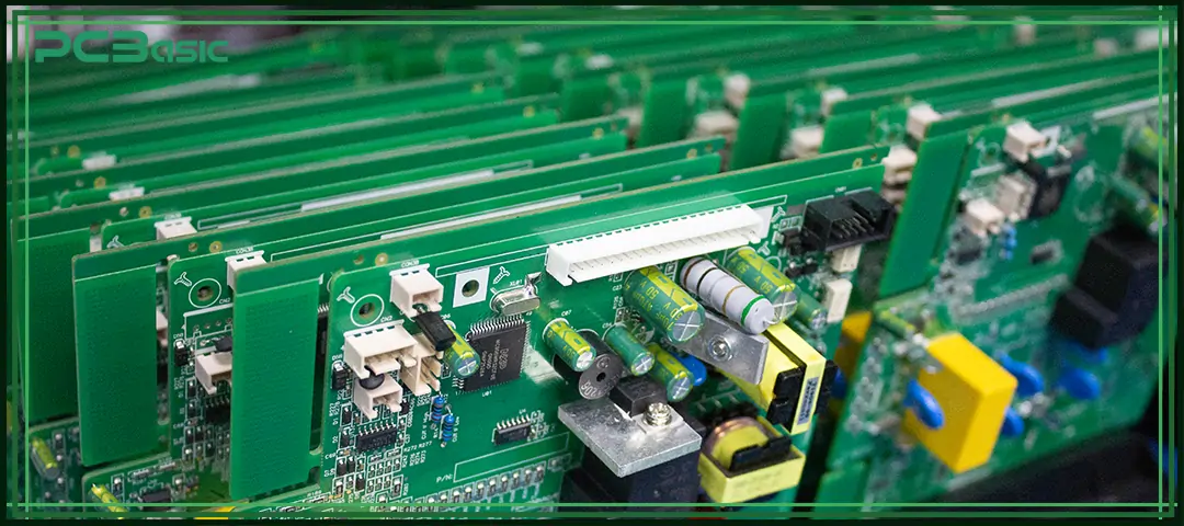
Before introducing the PCB assembly process, it is necessary to first clarify the difference between PCB fabrication and PCB assembly. These are two consecutive but distinct stages in electronic production.
PCB fabrication refers to the process of transforming a design drawing into a real circuit board. Its main tasks include:
• Etching copper traces to form electrical pathways
• Laminating multiple layers to support complex circuit structures
• Drilling holes and creating vias to connect different layers
• Applying surface finishes to improve solderability for later assembly
After completing these steps, we obtain a bare PCB board without any components installed. At this point, the circuit board still cannot function because it is merely a carrier and has no electronic function.
PCB assembly is the process of mounting and soldering electronic components onto a pre-made circuit board. It mainly includes
• Applying solder paste to the pads
• Placing components using automated equipment
• Performing reflow soldering or wave soldering to secure the components to the board
• Inspecting and testing the finished board
Without electronic components assembly, a PCB is just an empty shell. Only after going through the printed circuit board assembly process does the circuit board truly have a "nervous system", which can be powered on to operate and achieve practical functions.
In order to successfully complete PCB assembly manufacturing, the preparation of files and data in the early stage is crucial. If the data is incomplete or inaccurate, errors are likely to occur in the subsequent component placement and soldering.
When providing printed circuit board assembly services, it is usually necessary to prepare Gerber files, Bill of Materials (BOM), pick-and-place files (Pick-and-place / CPL / centroid files), NC drill files, and solder paste stencil files (Solder paste stencil file).
Different files provide different types of key information:
• Gerber files: define the PCB structure, including copper layers, solder mask, silkscreen, and solder paste layers
• BOM files: list reference designators, quantities, manufacturer part numbers, and package types
• Pick-and-place files: specify the X/Y coordinates of each component, its rotation angle, and whether it is mounted on the top or bottom side
When used together, these data can ensure the accuracy of electronic PCB assembly and avoid problems such as incorrect placement, reverse installation or missing components.
Before production begins, a DFM review (Design for Manufacturing) is required to ensure that the design is suitable for assembly manufacturing. The review mainly checks component spacing, pad sizes, component orientation, selected materials, and any potential manufacturing risk points.
Through DFM audits, problems can be identified and modified in a timely manner before production, thereby reducing scrapping and rework during the PCB board assembly process and avoiding unnecessary additional costs at the same time.
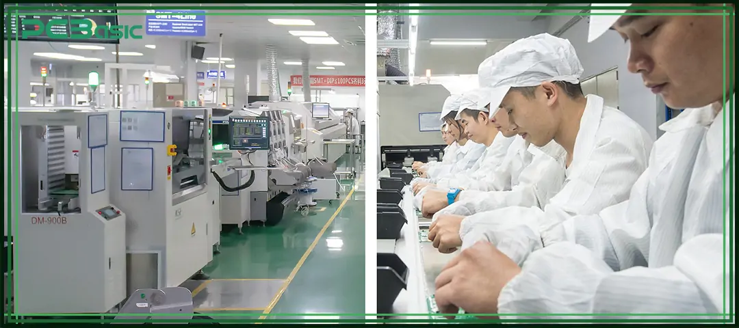
Depending on the application scenarios and performance requirements of different products, PCB assembly uses different process technology solutions to meet the demands of precision, strength and reliability.
Surface mount technology (SMT) is a process method that directly mounts components on the surface of a PCB. This technology can support high-density circuit design, making the product smaller in size and more compact in structure. At the same time, it is also very suitable for automated production lines, achieving high-efficiency circuit board assembly.
Due to its high precision, fast speed and strong adaptability, SMT has become the most fundamental and widely used core process in current electronic circuit board assembly.
Through-hole (THT) technology involves inserting component leads into pre-drilled holes on a PCB and then soldering and fixing them on the opposite side of the circuit board. This method can provide stronger mechanical support for components, featuring higher structural stability and durability.
Therefore, THT is typically used in connectors, transformers, and components that need to withstand significant mechanical stress. It still holds an important position in industrial PCB assembly.
Mixed technology assembly is a method that combines SMT and THT processes in a single board. It is suitable for complex circuit boards that require both high-precision mounting and strong mechanical fixation capabilities. This solution can simultaneously leverage the high-density advantage of SMT and the structural strength advantage of THT.
In PCB assembly and manufacturing, mixed assembly is widely used in fields such as industrial electronics and automotive electronics, and it is currently a very mature and practical assembly solution.
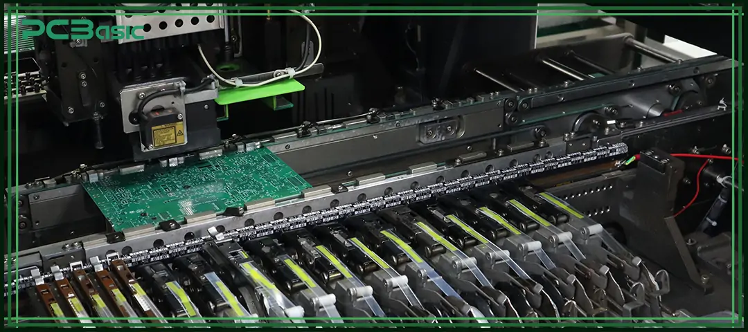
PCB assembly process starts from early-stage preparation, including BOM verification, component sourcing, machine programming, and incoming quality control (IQC). Before production, all components and materials must fully match the design requirements; otherwise, problems are likely to occur during subsequent mounting and soldering, affecting the overall quality.
The solder paste is accurately printed onto the PCB pads through a stainless-steel stencil. Whether the solder paste volume is appropriate directly determines whether the solder joints are firm. This step is the fundamental stage to achieve stable printed board assembly.
SPI equipment will detect the height and position of the solder paste to confirm whether the solder paste on each pad is uniform and whether the alignment is accurate. Through automated inspection, problems can be detected at an early stage to prevent defects from entering subsequent processes, thereby ensuring the stability of printed circuit assembly.
The automated pick-and-place machine quickly and accurately places components onto the PCB based on coordinate data. The built-in vision system of the device will check component type, polarity, and position. This process is not only fast but also highly accurate, and can maintain a consistent quality of electronic board assembly in mass production.
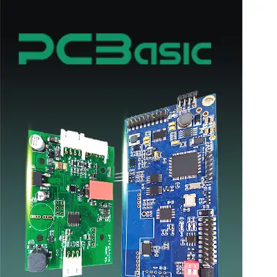
Time is money in your projects – and PCBasic gets it. PCBasic is a PCB assembly company that delivers fast, flawless results every time. Our comprehensive PCB assembly services include expert engineering support at every step, ensuring top quality in every board. As a leading PCB assembly manufacturer, we provide a one-stop solution that streamlines your supply chain. Partner with our advanced PCB prototype factory for quick turnarounds and superior results you can trust.
The assembled PCB will enter the reflow oven and be heated under the set temperature curve to melt the solder paste and form strong solder joints. Whether the temperature control is reasonable is important to the quality of solder joints and the safety of components. A good reflow soldering process is an important factor to ensure the long-term reliable operation of the PCB assembly process.
Inspections will be carried out both before and after reflow soldering. AOI is used to check whether the component placement is correct and whether the solder joints are qualified. X-ray is used to detect solder joints, such as BGA, that are invisible to the naked eye. Manual inspection deals with some special or complex situations. These inspection steps can identify problems in a timely manner and ensure the overall quality of PCB assembly manufacturing.
For components that require stronger mechanical fixation, wave soldering, selective soldering, or manual soldering methods will be adopted to complete the installation of THT components. This process is very common in circuit board assembly services for industrial products and is suitable for components such as connectors and power devices.
After the soldering is completed, it is necessary to remove the residual flux and impurities on the surface of the circuit board. This can not only improve the appearance but also enhance the electrical insulation performance and long-term stability, making the PCB assembly process more suitable for long-term use.
Confirm whether the circuit board can work normally through various testing methods, including In-Circuit Testing (ICT), Functional Testing (FCT), and burn-in testing for high-reliability products. Only the circuit boards that pass these tests can enter the next step of the PCB assembly manufacturing process.
In some special applications, a protective coating or potting is applied to the surface of the PCB to prevent moisture, dust, chemicals and vibration from affecting the circuit board. This type of process is often used for industrial PCB assembly and products in harsh environments.
After testing is completed, the PCB will be integrated into its enclosure, labeled with serial numbers or traceability markings, and packaged using anti-static materials for shipment. At this point, the circuit board is transformed from a bare PCB to a complete product, and the entire PCB assembly process is thus completed.
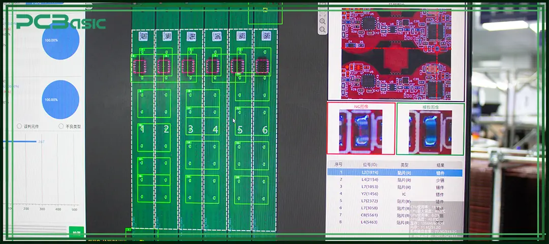
Quality control is the core part of the printed circuit board assembly process. Common quality control and inspection methods include:
• AOI (Automated Optical Inspection)
• X-ray inspection
• ICT (In-Circuit Testing)
• Functional testing
• Manual inspection
• Rework and repair process
Through these inspections and quality control methods, the product reliability, functional consistency and compliance with relevant standards and specifications in the PCB assembly and manufacturing process can be effectively ensured.
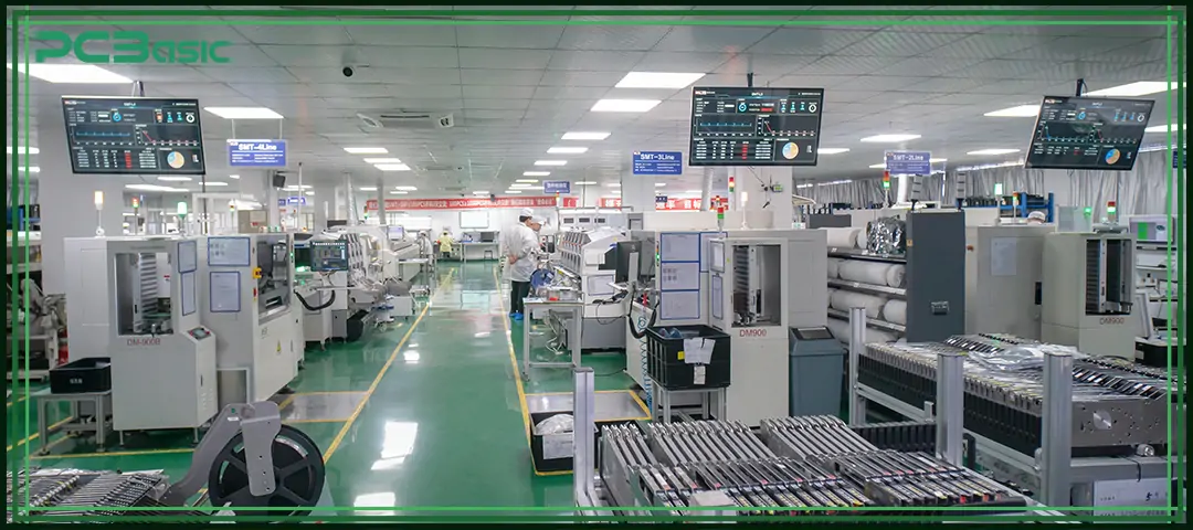
As a professional PCBA manufacturer, PCBasic has established a standardized management system from engineering review to inspection and delivery around the PCB assembly process to ensure the stability and consistency of PCBA.
• Review Gerber, BOM, and pick-and-place files for completeness
• Perform DFM (Design for Manufacturing) analysis
• Identify potential assembly risks early to reduce rework and scrap
• Improve feasibility in PCB assembly manufacturing
• Operate standardized PCB assembly lines
• Support SMT, THT, and mixed-technology assembly
• Ensure accuracy and efficiency in electronic PCB assembly
• Accommodate small-batch and high-mix production
• AOI for component placement and solder joint inspection
• X-ray inspection for BGAs and hidden solder joints
• ICT and functional testing for electrical verification
• Apply controlled rework and repair procedures when required
• Optional conformal coating and special processes
• Functional and burn-in testing support
• Meet the requirements of industrial PCB assembly
• Enhance long-term operational reliability
• Provide reliable printed circuit board assembly services
• Balance quality, lead time, and cost
• Support smooth transition from prototype to mass production
The PCB assembly process is the most crucial fundamental part of the electronic product manufacturing. From solder paste printing, component soldering, to inspection and final packaging, each step will directly affect whether the product can operate stably and its service life.
A full understanding of PCB assembly and manufacturing can help engineers and manufacturing teams achieve more stable product quality, a faster production pace, lower risks of errors and rework in actual production, and make it easier to realize batch and large-scale production.
Whether it is consumer electronics or industrial PCB assembly with higher reliability requirements, as long as the printed circuit board assembly process is properly controlled, the design plan can then be smoothly transformed into reliable and long-term usable finished products.
What is PCB assembly?
PCB assembly is the process of mounting and soldering electronic components onto a fabricated board to create a functional electronic device.
What is the difference between SMT and THT?
SMT mounts components on the surface, while THT inserts components through holes for stronger mechanical support.
How long does PCB assembly take?
Time depends on complexity and volume. Prototypes may take 1–2 days, while large production runs require longer lead times.
What affects PCB assembly cost?
Cost is influenced by board complexity, component types, inspection requirements, and whether SMT, THT, or mixed technology is used.
Why is inspection critical in PCBA?
Inspection ensures proper solder joints, correct placement, and electrical performance, preventing failures and costly recalls in electronic circuit board assembly.
Assembly Enquiry
Instant Quote
Phone contact

+86-755-27218592
In addition, we've prepared a Help Center. We recommend checking it before reaching out, as your question and its answer may already be clearly explained there.
Wechat Support

In addition, we've prepared a Help Center. We recommend checking it before reaching out, as your question and its answer may already be clearly explained there.
WhatsApp Support

In addition, we've prepared a Help Center. We recommend checking it before reaching out, as your question and its answer may already be clearly explained there.