Global high-mix volume high-speed PCBA manufacturer
9:00 -18:00, Mon. - Fri. (GMT+8)
9:00 -12:00, Sat. (GMT+8)
(Except Chinese public holidays)
Global high-mix volume high-speed PCBA manufacturer
9:00 -18:00, Mon. - Fri. (GMT+8)
9:00 -12:00, Sat. (GMT+8)
(Except Chinese public holidays)
HomePage > Blog > Knowledge Base > Solder Mask Expansion: A Complete Guide
Solder mask expansion represents a fundamental PCB design parameter that directly impacts manufacturing quality and reliability. Solder mask expansion refers to the space between a copper pad or trace edge and the matching solder mask opening edge. This intentional solder mask opening expansion around the PCB pads provides for full pad exposure upon soldering and accommodates possible manufacturing misalignments.
During PCB fabrication, perfect alignment between layers rarely occurs. Consequently, the solder mask openings may shrink or become slightly misaligned from their intended positions. Without adequate expansion, these misplacements can actually result in solder mask overlap on pads, either partially or fully, leading to faulty connections and unstable solder joints. The expansion setting can be defined universally through design rules or adjusted individually for specific pads or vias as needed. In high-density designs, precise tuning is especially critical in order to balance exposure of the pads against sufficient solder mask between features.
In PCB manufacturing, solder mask expansion defines the gap between a copper pad’s edge and its surrounding mask opening. It affects soldering quality, component adhesion, and circuit reliability.

Solder mask expansion is specifically defined as the radial distance by which a solder mask opening protrudes outside (or shrinks inside) the copper pad or via to which it pertains. This measurement is therefore positive or negative:
● Positive expansion: Creates a mask opening larger than the copper pad, which is standard for most applications
● Negative expansion: Results in a mask opening smaller than the copper pad, used for partial tenting
When measuring solder mask expansion, designers must first establish the reference point. The expansion can be calculated from either:
1. The pad/via land perimeter (copper edge): This is the default reference in most design software
2. The hole edge: When enabled, calculations use the pad/via hole perimeter instead
For example, a 5 mil expansion on a 60 mil round pad results in a 70 mil mask opening (60 mil + 2 × 5 mil). If the same pad has a 30 mil hole and expansion is referenced from the hole edge, a 20 mil expansion also yields a 70 mil opening.
Measurement accuracy becomes particularly important for high-density designs. In modern PCB design software, expansion values are typically specified separately for top and bottom layers through:
● Expansion top: The value applied to the initial pad/via shape to obtain the final shape on the top solder mask layer
● Expansion bottom: The equivalent parameter for the bottom layer

Most manufacturers recommend solder mask expansion between 2 to 5 mils, with 3 mils common to allow for 2 mils of misregistration. This helps prevent solder bridges and ensures reliable pad exposure.
Proper solder mask expansion plays a crucial role in PCB reliability, functionality, and manufacturing success. This deliberate design parameter affects everything from component connections to long-term device performance. Let's examine why this seemingly small detail demands careful attention.
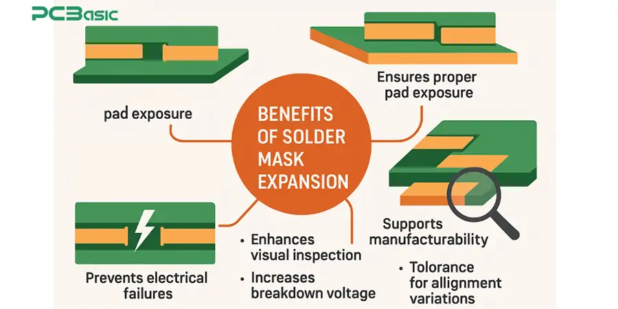
The primary purpose of solder mask expansion is to provide enough exposure of the pads for proper soldering. Without expansion, the manufacturing tolerances will cause the mask to overlap pads, thus reducing the area available for soldering and degrading the contact integrity. Proper expansion facilitates solder bonding on all pad sides, which is particularly important for fine-pitch packages like QFN and LGA, thus providing proper placement and good electrical contacts.
Effective solder mask expansion improves circuit reliability by avoiding solder bridging and short circuits during assembly. It also avoids oxidation of copper traces, maintaining their electrical characteristics and ensuring long-term performance.
Notably, proper mask expansion also:
● Enhances the visual inspection capabilities for quality control
● Increases the breakdown voltage of the dielectric layer
● Prevents the growth of whiskers that could cause short circuits
From a manufacturing perspective, solder mask expansion provides crucial tolerance for alignment variations, compensating for common misregistrations between the mask and copper features. Proper expansion prevents defects and costly rework, while overly tight values may require error-prone manual clearance adjustments. A typical expansion of 2–4 mils balances pad exposure with manufacturing reliability.
Standard solder mask expansion values exist as guidelines rather than strict rules, varying based on manufacturing capabilities and design requirements. Throughout the industry, manufacturers and designers use established ranges that balance proper pad exposure with manufacturing practicality.

The industry standard for solder mask expansion typically ranges from 2 to 5 mils (0.002"–0.005"). Many fabricators default to 4 mils, though this can vary with specific processes. For high-precision or high-density designs, smaller expansions—often 0 to 1 mil—may be used, with the understanding that fabricators may adjust these values. A commonly recommended minimum is 3 mils per side, which compensates for about 2 mils of misregistration, helping prevent solder mask from covering pad surfaces. Most PCB design tools reflect these standards, with rule-based defaults often set to 4 mils.
PCB manufacturers typically provide their own guidelines based on their fabrication processes and equipment capabilities. These recommendations consider factors such as:
● Manufacturing process precision (silk screen, Liquid Photo-Imageable, or laser direct imaging)
● Component lead pitch requirements
● Minimum solder mask sliver capabilities
High-quality fabricators can achieve 2.5 mil expansions with 3 mil webs, while others may require larger values. Fine-pitch components (0.5 mm or smaller) may use 2 mil expansion, though it can increase cost. Expansion needs also depend on board type—high-frequency or high-power boards often need larger clearances, while dense layouts need tighter control. Designers typically allow a ±3 mil adjustment range in fabrication drawings.
The relationship between minimum solder mask expansion and sliver represents a critical balance in PCB design that directly affects manufacturing reliability and functionality.
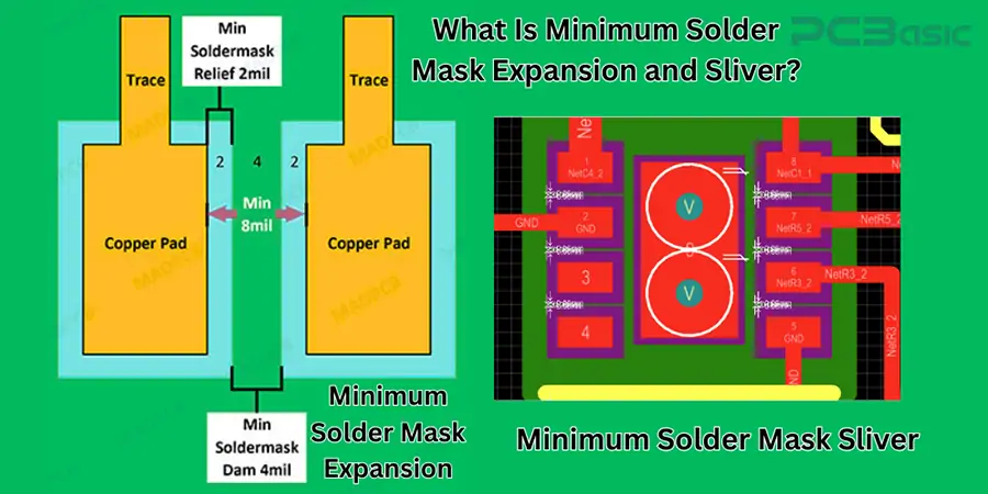
Minimum solder mask expansion is the smallest allowed gap between a copper pad and its solder mask opening. It’s critical in high-density designs where space is limited. For fine-pitch components like 0.4 mm pitch BGAs with ~250 μm balls, pads are typically sized at 80% of the ball diameter. A typical starting point is 3 mils per side, which compensates for approximately 2 mils of potential misregistration. However, in tight layouts, this may need to be reduced to avoid violating solder mask sliver requirements.
Minimum solder mask sliver is the narrowest allowable width of mask between adjacent openings. If too narrow, it can cause manufacturing issues. Most standards set this minimum between 3–4 mils (75–100 microns).
When solder mask slivers become too thin, several issues may arise:
● The thin mask section might flake off during manufacturing
● Solder might flow across the thin sliver, creating bridges on top of the solder mask
● Solder could wick along copper between openings, compromising electrical connections
These concerns explain why PCB design rule checks enforce minimum solder mask openings. Though some fabricators allow 2.5 mil slivers, 4 mils is a safer standard. Designers must balance adequate mask expansion with enough sliver width, especially in fine-pitch and high-density layouts.
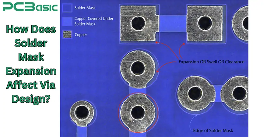
Via design represents a critical consideration when applying solder mask expansion in PCB manufacturing. Unlike component pads, vias present unique challenges that demand careful attention to mask parameters. Vias in PCB designs can be treated in several ways regarding solder mask:

It is important to treat vias correctly in solder mask design to avoid solder wicking, which can weaken joints. Tented vias require proper expansion to control solder flow, while tented vias require negative expansion for full coverage. For partially tented vias, the expansion should be close to the via hole; for fully tented ones, it must be negative and at least equal to the via or pad radius.
When vias are close to SMD pads, designers must ensure sufficient dam width and carefully manage mask expansion to avoid solder migration. Leaving one end of a via open helps prevent trapped volatiles during reflow. Tenting both sides is usually fine for small vias, but partial exposure may be better for larger ones.
Tented vias can limit test access, so it's common to mask ground vias and keep power or signal vias uncovered for probing.
Proper use of solder mask expansion in PCB designs involves technical knowledge and cautious handling using design software. Contemporary PCB design software provides a range of facilities for appropriate handling of this valuable parameter.
Starting the solder mask expansion process is achieved by going to the design rules section of your PCB program. For Altium Designer, it is located under "Design > Rules" in the PCB Rules and Constraints Editor, where global and component-specific expansion rules are defined. The program allows for setting the top and bottom layers separately in some fields by the titles "Expansion top" and "Expansion bottom."

One major choice is choosing the point of reference for your expansion. In defining the rules, you need to decide if you want to measure expansion from:
● The pad/via land perimeter (copper edge)
● The hole edge (when enabled via "Solder Mask From The Hole Edge" option)
For instance, a 5 mil expansion applied to a 60 mil diameter round pad creates a 70 mil opening when measured from the pad edge. The same opening would be a 20 mil expansion when measured from the edge of a 30 mil hole.
To tent vias partially or completely:
● For partial tenting (covering land area only): Set expansion negative to close the mask to the hole (land perimeter reference), or 0 (hole edge reference).
● For complete tenting: Use negative expansion equal to or larger than the pad/via radius.
Individual components can be fine-tuned step by step using the Properties panel by overriding the design rules or by tenting, hence allowing optimization towards general and high-density regions.
Along with design rules, mask expansion verification through visualization tools aids in detecting problems prior to manufacturing. It is recommended to speak with the PCB manufacturer because they can give details regarding their capabilities and procedures. Designers have been known to add comments to fabrication drawings to specify solder resist openings within a standard tolerance of ±3 mils.
Solder mask expansion is usually neglected but it plays an important role in PCB manufacturability, operability, and reliability. A usual range of 2–5 mils is a trade-off between optimal values and feasible manufacturing limits, particularly in high-density layouts. Designers need to take optimum values and feasible manufacturing limits into consideration.
New PCB tools provide fine-grained control of expansion settings, global constraints, and localized adjustments. Options such as via tenting show how the settings influence performance and assembly. 3–4 mils is conventional, but the best value is based on particular manufacturing and design requirements, which means close communication between the designer and the manufacturer.
 About PCBasic
Time is money in your projects – and PCBasic gets it. PCBasic is a PCB assembly company that delivers fast, flawless results every time. Our comprehensive PCB assembly services include expert engineering support at every step, ensuring top quality in every board. As a leading PCB assembly manufacturer, we provide a one-stop solution that streamlines your supply chain. Partner with our advanced PCB prototype factory for quick turnarounds and superior results you can trust.

Assembly Enquiry
Instant Quote
Phone contact

+86-755-27218592
In addition, we've prepared a Help Center. We recommend checking it before reaching out, as your question and its answer may already be clearly explained there.
Wechat Support

In addition, we've prepared a Help Center. We recommend checking it before reaching out, as your question and its answer may already be clearly explained there.
WhatsApp Support

In addition, we've prepared a Help Center. We recommend checking it before reaching out, as your question and its answer may already be clearly explained there.