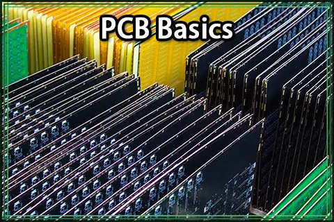
As we all know, printed circuit boards (PCBs) are the core and backbone of modern electronic devices. From smartphones and computers to household appliances and industrial equipment, we encounter circuit boards almost every day. A circuit board not only houses various key electronic components but also provides stable communication channels between these components, serving as the foundation for the normal operation of equipment. However, although PCBs support every aspect of our modern life, many people seldom truly think about the technical principles that drive them.
In this basic knowledge of PCBs, we will delve into what a PCB is in electronics, understand its composition and common terms, analyze various types of PCBs, and explain how these PCB components are combined to form the backbone of modern electronic products. This tutorial is intended as a PCB design 101 introductory material to establish a clear PCB basics for beginners and help us better understand the world of electronics.

What is a PCB?
A PCB is a thin board made of insulating materials such as fiberglass board, on which conductive pathways are etched or printed. These circuits enable the current to flow between different PCB components. In simple terms, circuit boards are the skeleton and nervous system of electronic products.
The history of the PCB can be traced back to the early 20th century. At that time, point-to-point wiring was commonly used, where wires were soldered one by one to the connection points. Later, the wire wrapping emerged, which enhanced reliability by tightly winding thin wires around connection posts. However, as vacuum tubes and relays are gradually replaced by silicon chips and integrated circuits. Additionally, the demand for miniaturization, low cost and high reliability is becoming increasingly strong, which has driven the popularization of PCBS.
During World War II, military equipment required smaller and more reliable circuits, and as a result, PCB technology developed rapidly. After the war, especially between the 1950s and 1970s, PCBs began to be mass-produced and became the core of consumer electronics, computers and communication equipment. Meanwhile, multilayer PCB technology had gradually matured, making circuit design more compact and efficient.

Basic PCB Composition
Each PCB is composed of different materials and layers, which together form a reliable circuit platform. For those who are just starting to learn PCB basics or get in touch with PCB design 101, understanding this basic PCB composition is the first step to recognizing the working principle of circuit boards.
FR4 Substrate

The base material of most PCBs is FR4, which is a fiberglass-reinforced epoxy laminate. It can provide strength, durability and insulation. For circuit boards, FR4 is like the foundation of a house, used to support all PCB components.
Copper Layer

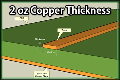
FR4 is covered with a thin layer of copper. Through etching, the copper is made into precise conductive traces, which are used to connect various components and transfer current. The thickness of the copper layer is very important as it determines how much current the circuit board can carry and affects the overall performance.
Soldermask

The most recognizable feature of a PCB is its colored coating, which is the soldermask. The common one is green, but it can also be blue, red or black. The soldermask can protect the copper circuit from oxidation and also prevent solder bridges during soldering. It also makes the circuit board look cleaner and more professional.
Silkscreen

The silkscreen is the layer of white text and symbols printed on the surface of the circuit board, used to label the names and positions of components, helping to install and troubleshoot PCB components more easily. Silkscreen is like a map that can clearly tell us where the components should be placed.
We can say that the substrate, copper layer, soldermask and silkscreen layer together form a complete PCB. They not only provide physical support but also establish electrical pathways and make circuit boards easier to assemble and identify.
Printed Circuit Board Types
According to different structures, materials, electrical properties and applications, we can classify circuit boards into the following four types:
By Number of Layers
Single-Sided PCB
It is the simplest PCB that has only one layer of copper, with components concentrated on one side. These PCBs have low cost and simple structure, and are often used in basic electronic products such as radios, toys and calculators.
Double-Sided PCB
Both sides of the double-sided board are covered with copper, and the circuits on the two sides are connected through via holes. Double-sided boards have a wide range of applications, such as in home appliance control boards, lighting equipment, industrial control systems, etc.
Multilayer PCB
This type of board is composed of three or more layers of copper stacked together, with an insulating layer in between. They can achieve more complex and compact designs and are often used in computer motherboards, communication equipment, and medical electronics.
By Material
Rigid PCB

It is the most common type of PCB with hard materials such as FR4 (glass fiber epoxy resin) as the base material, and it cannot be bent. It is widely used in computers, televisions and electronics.
Flexible PCB, FPC

It can be bent and folded with PI (polyimide) or PET as the base material. It is commonly found in mobile phones, cameras and wearable devices.
Rigid-Flex PCB

Combining rigid and flexible boards, it offers both strength and flexibility. It is commonly used in aerospace systems, medical electronics, and high-reliability equipment.
By Electrical Performance
High-Frequency PCB
It uses special materials such as PTFE (Teflon) and supports high-speed signal transmission. It is applicable to RF circuits, radars, satellite communications and 5G equipment.
Power PCB
Its copper is thicker (such as 2oz, 3oz and above) and can carry large currents. This type of PCB is commonly found in automotive electronics, power equipment, and industrial control.
HDI PCB
By using microvias, blind vias, buried vias and other processes, the routing is denser. It is often used in small high-performance products such as smartphones and tablet computers.
By Application
Consumer Electronics PCB
Used for mobile phones, computers, televisions and household appliances.
Automotive PCB
It is used for engine control units, ADAS (Advanced Driver Assistance Systems), vehicle lighting and in-vehicle entertainment systems.
Industrial Control PCB
Used for factory automation, robots, sensors, etc.
Medical PCB
It is used for electrocardiogram monitors, diagnostic equipment, and implantable medical devices.
Aerospace/Defense PCB
It is used in satellites, radars, avionics and military communication systems.
The Circuit Board Components List
When understanding a PCB, we also need to know what components are on the circuit board and their functions. Different circuit board components are responsible for different functions like connecting, controlling, protecting or processing signals. Together, they determine whether the entire electronic device can work stably and reliably. Below, we will introduce common circuit board components from several main categories.
Mechanical Components
Mechanical components are mainly used to provide structural support and auxiliary functions, which can enhance the overall stability and mechanical strength of the PCB. Typical mechanical components include:
• Connectors: used to connect the circuit board with other circuits or external devices.
• Mounting Holes: used to fix the circuit board so that it can be securely installed in a case or device.
• Heat Sinks: help components such as power transistors and voltage regulators dissipate heat quickly, ensuring the circuit works within a safe temperature range.
Electrical Components
Electrical components are mainly responsible for transmitting electrical energy and helping circuits in achieving input, output and protection. They mainly ensure a stable power supply and circuit safety. Common electrical components include:
• Switches: Used to control whether a circuit is on or off.
• Relays: Used for automatic control or isolation in circuits.
• Fuses: Provide overcurrent protection; when the current is too high, they melt and cut off the circuit to protect it.
Passive Components
Passive components do not actively generate or amplify signals but store, distribute or limit electrical energy. This type of component is the most common one on circuit boards.
• Capacitors (C): Units are usually μF (microfarads) or mF (millifarads). A capacitor stores charge between two conductors separated by an insulator, mainly used for filtering, coupling, or temporary energy storage.
• Resistors (R): Units are ohms (Ω). Their function is to limit current. Different resistance values control current levels. Resistors usually have colored bands to indicate resistance value.
• Inductors (L): Units are henry (H). An inductor is a coil that generates a magnetic field and stores energy when current flows through it. They are commonly used in filtering and noise suppression.
Active Components
Active components can control, amplify or generate electrical signals and are the core of circuits.
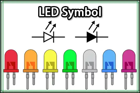
• Diodes: Represented by the letter "D", they can only conduct current in one direction and are often used to prevent reverse current from damaging circuits. Light-emitting diodes (LEDs) can not only conduct electricity but also emit light.
• Transistors: They can amplify signals or act as a switch and are one of the core components of modern electronic products. The common types include NPN and PNP bipolar transistors.
• Integrated Circuits (IC): Known as the "brain" of circuit boards, they integrate components such as transistors, resistors, and capacitors internally, and are used for signal processing and logic control.
Other Circuit Board Components
In addition to the above-mentioned types, there are also some special functional components:
• Crystal Oscillator: It provides precise and stable clock signals and is commonly found in microcontrollers and computer motherboards.
• Thyristors (SCRs): Composed of four layers of silicon material, they combine the features of diodes and transistors and are often used in high-current and high-voltage switching control.
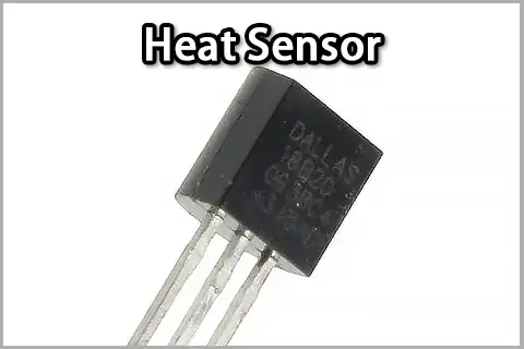
• Sensors: They convert physical quantities such as light, temperature, humidity and pressure into electrical signals and are an important part of smart electronic products.

About PCBasic
Time is money in your projects – and PCBasic gets it. PCBasic is a PCB assembly company that delivers fast, flawless results every time. Our comprehensive PCB assembly services include expert engineering support at every step, ensuring top quality in every board. As a leading PCB assembly manufacturer, we provide a one-stop solution that streamlines your supply chain. Partner with our advanced PCB prototype factory for quick turnarounds and superior results you can trust.
Terminology Related to a PCB
Finally, let's take a look at some professional terms frequently encountered in the PCB industry:
Annular Ring – The copper ring around a drilled hole. It makes sure the hole stays connected to the circuit.

DRC (Design Rule Check) – A check done by PCB software. It looks for design errors like spacing that’s too close.

Drill Hit – How accurate the drilled hole is compared to the design. Good accuracy means parts fit correctly.

Finger – Exposed copper at the board edge. It lets the PCB plug into another device, like a card slot.

Mouse Bites – Small holes in a row on the board edge. They make it easy to snap PCBs apart after production.

Pad – A copper spot where parts are soldered. Every component needs a pad to connect to the board.

Panel – A big board that holds many smaller PCBs. It helps speed up manufacturing.

Paste Stencil – A thin metal sheet with holes for pads. It is used to print solder paste on the board.

Pick-and-Place – A machine that quickly puts components onto the PCB. It’s faster and more accurate than by hand.

Plane – A large copper area, usually for ground or power. It keeps the circuit stable and reduces noise.

Plated Through Hole (PTH) – A hole with metal inside. It connects signals between layers of the board.

Pogo Pin – A spring pin used for testing. It touches the board without damaging it.

Reflow – The heating step that melts solder paste. This makes the parts stick permanently.

Silkscreen – Printed text or marks on the PCB. It shows where parts go and helps with assembly.

Slot – A cut or opening in the board. It is used for connectors or special shapes.

Solder Paste – A gray paste with tiny solder balls. It is used before reflow to attach components.

Solder Pot – A bath of hot liquid solder. Boards are dipped into it to solder through-hole parts.

Soldermask – The colored coating on the PCB, often green. It protects copper and stops short circuits.

Solder Jumper – When solder accidentally connects two pads. It causes a short and must be fixed.

Surface Mount – A way to place parts directly on the surface. It allows smaller and lighter electronics.

Thermal – A copper design that helps with heat. It improves cooling and makes soldering easier.

Thieving – Extra copper added during production. It keeps copper plating even across the board.

Trace – The copper line that carries current. It is like a wire on the PCB.

V-Score – A V-shaped cut in the board. It makes breaking panels apart easier.

Via – A small plated hole that connects board layers. It lets signals travel between layers.

Wave Solder – A process where parts are soldered by passing the board over flowing solder.

BOM (Bill of Materials) – A complete list of all components needed for the PCB. It tells the factory exactly what to buy and use.

Gerber Files – The standard file format for PCB manufacturing. They tell the factory how to make copper layers, holes, and silkscreen.

Copper Pour – A large filled area of copper. It helps with grounding and heat dissipation.

Trace Width – The thickness of a copper line. It decides how much current it can safely carry.

Clearance – The minimum space between two copper features. Good clearance prevents short circuits.

Stack-up – The order of layers in a multilayer PCB. It affects performance and cost.

Impedance Control – Adjusting trace width and spacing for high-frequency signals. It makes sure signals travel correctly.

Blind Via – A via that starts on the surface but doesn’t go through the whole board.

Buried Via – A via hidden inside the layers, not visible on the outside.

Test Point – A small pad or hole used to check signals or power during testing.

Fiducial – Small reference marks on the PCB. Machines use them to align components accurately.

Edge Connector – A set of copper fingers on the edge of the board. Often used in computer cards and plug-in modules.

Copper Weight – The thickness of the copper layer, usually measured in ounces per square foot.

SMD (Surface Mount Device) – A component designed for mounting directly on the board surface.

THT (Through-Hole Technology) – A component with pins that go through holes in the PCB.

Via-in-Pad – A via placed directly inside a pad. It saves space but needs extra care to manufacture.

Designing Your First PCB (Beginner Tips)
When we first start learning PCB design, we may find the process very complicated. But if it is broken down into several small steps, it will be much easier. Here are some practical suggestions for beginners to help us complete the design of our first printed circuit board.
Choose CAD Software
The first step is to select a PCB design software.
• KiCAD: Free and open source, ideal for students and hobbyists.
• Eagle: Simple interface with plenty of online tutorials, making it easy to get started.
• Altium Designer: More powerful, widely used in professional engineering teams, and provides rich, advanced design tools.
Start from Schematics
Don't directly draw the PCB layout right from the start. We can first draw the circuit schematic diagram. A schematic diagram is like a blueprint for a project, clearly showing the connection relationships among various components. Once the schematic diagram is confirmed to be correct, we will be more confident when moving on to PCB design.
Learn from Open Source Designs
One good way to learn is to refer to existing open source PCB projects. Many electronic enthusiast communities share their board designs. By studying these layouts, we can learn how they are wired, place components, and handle power and ground levels. This can help us avoid common mistakes and also provide us with practical design references.
Accept Mistakes as Inevitable
Our first PCB is almost certain to have problems - such as incorrect component placement, crossed traces, or inappropriate pad sizes. This is very normal. Treat the first design as an exercise rather than the final product. As our experience accumulates, we will keep making progress, and our understanding of PCB design rules will become increasingly profound.
Practice with Simple Projects
Before attempting complex circuits, start with small projects, such as a small circuit board that can light up LEDs, an expansion board for temperature or motion sensors, or a small power module with a voltage stabilizing chip and capacitors. These projects are easy to make and have low costs, making them very suitable for practice.

Conclusion
Learning the basics of PCB is the first step into the electronic world. This guide provides a comprehensive introduction to what a PCB is, common types of PCBs, circuit board components, and some common terms used in PCB design and manufacturing.
For beginners in circuit boards, learning up to this point is just the beginning. After mastering these PCB components and terms, we still need to further understand CAD software, schematic design and simulation tools.