Global high-mix volume high-speed PCBA manufacturer
9:00 -18:00, Mon. - Fri. (GMT+8)
9:00 -12:00, Sat. (GMT+8)
(Except Chinese public holidays)
Global high-mix volume high-speed PCBA manufacturer
9:00 -18:00, Mon. - Fri. (GMT+8)
9:00 -12:00, Sat. (GMT+8)
(Except Chinese public holidays)
HomePage > Blog > Knowledge Base > What Is Silkscreen in PCBs?
In electronics manufacturing, PCB silkscreen does not participate in the transmission of electrical signals. However, it is very important for the design, assembly and later maintenance of PCBs, although many people do not pay attention to it. Silkscreen itself does not affect whether the circuit is conducting or not, but without it, engineers would have almost no idea where to start when assembling components, debugging circuits or repairing PCBs, which would be prone to errors and greatly reduce efficiency.
So, what exactly is silkscreen? Why can it be seen on almost every circuit board? In this article, we will explain PCB silkscreen from the following aspects: what it is, what materials are used, how it is printed, the common PCB screen printing methods, the PCB silkscreen guidelines to be noted during design, and what specific role it plays in PCB assembly and production.
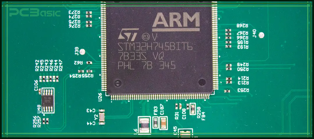
PCB silkscreen is a layer of non-conductive ink printed on the surface of a circuit board. It is used to mark important information such as component reference designators, test points, polarity indicators, warning symbols, company logos, version numbers and other identifiers. In simple terms, the white or yellow text, such as "R1", "C3" or the manufacturer's logo that you see on the circuit board is the PCB silkscreen.
It is also known as the legend, component legend or board markings. The silkscreen does not affect electrical performance, but it plays a crucial guiding role during assembly, inspection and maintenance of PCBs.
Although both the PCB silkscreen and the solder mask are located on the surface of the PCB, their functions and materials are completely different. Understanding the differences between the two helps to better understand the structure and manufacturing process of PCBs. The following table shows the core differences between them:
|
Feature |
PCB Silkscreen |
Solder Mask |
|
Purpose |
Text & labels |
Protects copper |
|
Material |
Epoxy ink |
Polymer resin |
|
Function |
Visual information |
Electrical insulation |
|
Example |
R1, C5, +/–, Pin 1 |
Green coating |
1. Component Identification
On PCBs, common silkscreen markings such as R1, C5, and U3 are used to quickly identify components like resistors, capacitors, ICs, connectors, jumpers, and LEDs. Without PCB silkscreen, engineers have to search for each schematic diagram one by one, which not only wastes time but is also prone to errors. With a clear PCB silkscreen, both assembly and later maintenance will be much efficient.
2. Assembly & Orientation Guidance
Silkscreen not only provides component numbers but also marks the orientation information of the components, such as the Pin 1 markers on ICs, the polarity symbols for diodes and electrolytic capacitors (+ / -), and outlines of components. These can effectively avoid reverse, misplaced or missing installation during assembly.
3. Testing and Troubleshooting
During the debugging or repair phase, technicians will find the test points (TP1, TP2), jumpers (J1, J2), adjustment pins or connector numbers through silkscreen. They can quickly determine the circuit position without referring to documentation, allowing issues to be located and resolved much faster.
4. Traceability & Documentation
PCB silkscreen can also be used to print the version number (such as V1.2), production batch, date code, company name or serial number of the circuit board. This information facilitates the control of the production process and also helps customers identify the source of the product during after-sales service or upgrades.
5. Aesthetic & Branding
A professional PCB not only has clear silkscreen printing but also includes the company logos, product name, QR code, anti-counterfeit markings, UL/CE/RoHS and other certifications. It is not only a functional description but also a part of the brand image, making the circuit board look more professional and trustworthy.
6. Safety Indicators
For PCBs containing high voltage, current or electrostatic-sensitive areas, PCB silkscreen is often used to remind users to pay attention to safety, such as High Voltage symbols, ESD warning, and ground symbols. These simple PCB silkscreen symbols can effectively reduce the risk of misuse and comply with safety standards and product regulations.
|
Category |
Examples |
|
Component Labels |
R1, R2, C5, U3 |
|
Orientation |
Pin 1 dots, “+” polarity marks |
|
Test Points |
TP1, TP2 |
|
Logos and Branding |
Company name, logo |
|
Compliance Symbols |
UL, CE, RoHS |
|
Safety Warnings |
High Voltage, ESD |
|
Connector Labels |
J1, P3, USB_TX, GND |
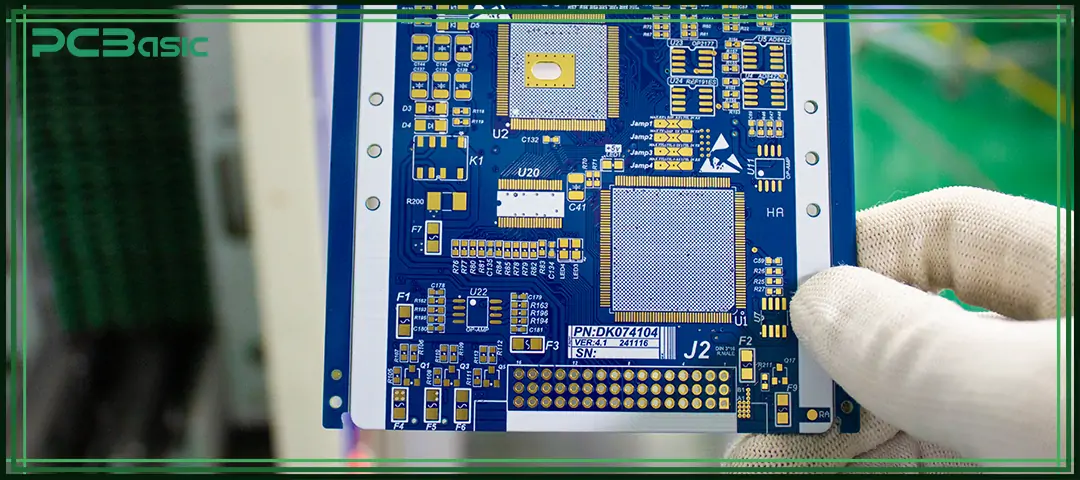
In PCB manufacturing, the ink used in PCB silkscreen is a non-conductive ink based on epoxy resin. This material has excellent adhesion and abrasion resistance. Even if the circuit board undergoes high-temperature soldering, cleaning or later assembly processes, the silkscreen remains clear and does not peel off easily.
To present different colors, special pigments are added to the ink. The most common one is white, but black or yellow can also be used according to the board color and visual requirements.
Meanwhile, an appropriate amount of solvent is added to the ink to control its viscosity and printing performance, ensuring that the characters are clear and do not spread. Some manufacturers also add additives such as UV resistance and chemical corrosion resistance to ensure that the screen printing remains stable during damp, thermal shock or cleaning processes.
|
Color |
Usage |
|
White |
Most common on green PCBs |
|
Black |
Used on white or aluminum PCBs |
|
Yellow/Red |
Less common, special-purpose |
The thickness of PCB silkscreen is usually 0.02-0.10 mm (20-100 μm). This thickness does not affect the component mounting or soldering process, but ensures that the text and symbols are clearly visible and have sufficient wear resistance.
Time is money in your projects – and PCBasic gets it. PCBasic is a PCB assembly company that delivers fast, flawless results every time. Our comprehensive PCB assembly services include expert engineering support at every step, ensuring top quality in every board. As a leading PCB assembly manufacturer, we provide a one-stop solution that streamlines your supply chain. Partner with our advanced PCB prototype factory for quick turnarounds and superior results you can trust.
In PCB manufacturing, PCB silkscreen can be printed in various ways, and different processes have their own advantages and disadvantages in terms of cost, precision, durability and efficiency. The following table compares the common PCB silkscreen printing methods, facilitating a quick understanding of the characteristics of each method.
|
Method |
Description |
Pros |
Cons |
|
Manual Screen Printing |
Mesh screen + squeegee |
Low cost |
Low accuracy |
|
Liquid Photo Imaging (LPI) |
Photo-sensitive epoxy + UV |
High precision |
More expensive |
|
Direct Legend Printing (DLP) |
Inkjet prints CAD data |
Fast, no stencil |
Less durable |
|
Dry Film |
Laminated photo film |
Thick & durable |
Higher cost |
|
Laser Direct Imaging |
Laser ablation |
No ink needed |
Very expensive |
Add a silkscreen layer in software such as KiCad, Altium Designer, Eagle or OrCAD for drawing information such as component reference designators, polarity labels, Pin 1 directions, etc.
After the design is completed, export the Gerber file, where the silkscreen usually includes GTO (Gerber Top Overlay) and GBO (Gerber Bottom Overlay) layers. These files are the standard formats for factories to identify silkscreen patterns. If they are missing, manufacturers will not be able to print silkscreen.
Traditional screen printing uses a stencil, and the position of the holes needs to be made according to Gerber. For digital methods like DLP (Direct Legend Printing), on the other hand, it directly uses CAD data without the need for a stencil. This step determines which printing method to use and the precision of screen printing.
Before silkscreen printing, the applying and curing of the solder mask must be completed first, which is commonly green ink.
Choose PCB screen printing, LPI or DLP processes as needed. The silkscreen pattern will be printed onto the surface of the PCB, providing text and symbols for subsequent assembly.
After the printing is completed, the ink needs to be cured through thermal curing or ultraviolet (UV) curing to prevent scratching or peeling. Insufficient curing may lead to problems such as smudging, fading, or peeling.
Automated Optical Inspection (AOI) is used to check if the silkscreen is correctly applied. Key checks include whether PCB silkscreen symbols are complete, whether alignment is accurate, whether text is clear and readable or whether it follows PCB silkscreen guidelines.
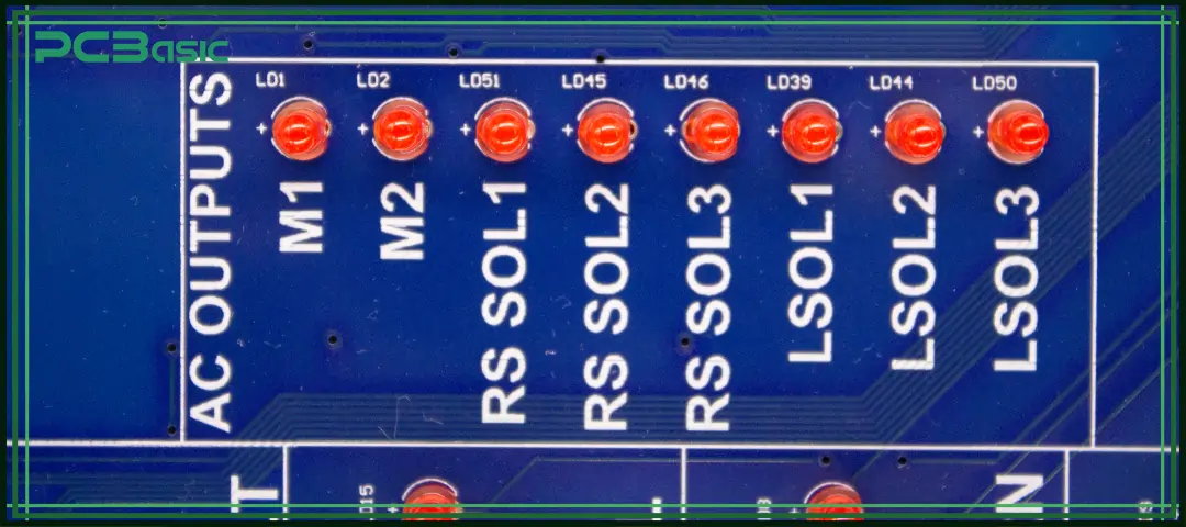
Although PCB silkscreen is just a small detail on the circuit board, it plays a crucial role. It does not affect the electrical function of the circuit, but it determines whether the components can be mounted correctly, assembly efficiency is improved, debugging is convenient, document records are standardized, and whether the overall appearance of the PCB is professional.
Understanding what silkscreen is in PCBs, the materials used for silkscreen, the production process, and the PCB silkscreen guidelines is the basic knowledge that every electronic engineer, PCB designer or manufacturer should master.
Q1: What is silkscreen in PCB?
It is a printed layer of ink used to label components, symbols, and markings.
Q2: Is PCB silkscreen necessary?
Yes — without it, assembly and maintenance become harder and error-prone.
Q3: What is the difference between solder mask and silkscreen?
Solder mask protects copper; silkscreen on PCB adds labels and guidance.
Q4: What is used in PCB silkscreen materials?
Epoxy-based ink is resistant to heat and chemicals.
Assembly Enquiry
Instant Quote
Phone contact

+86-755-27218592
In addition, we've prepared a Help Center. We recommend checking it before reaching out, as your question and its answer may already be clearly explained there.
Wechat Support

In addition, we've prepared a Help Center. We recommend checking it before reaching out, as your question and its answer may already be clearly explained there.
WhatsApp Support

In addition, we've prepared a Help Center. We recommend checking it before reaching out, as your question and its answer may already be clearly explained there.