Global high-mix volume high-speed PCBA manufacturer
9:00 -18:00, Mon. - Fri. (GMT+8)
9:00 -12:00, Sat. (GMT+8)
(Except Chinese public holidays)
Global high-mix volume high-speed PCBA manufacturer
9:00 -18:00, Mon. - Fri. (GMT+8)
9:00 -12:00, Sat. (GMT+8)
(Except Chinese public holidays)
HomePage > Blog > Knowledge Base > PCB Edge Connectors: Design, Manufacturing and Uses
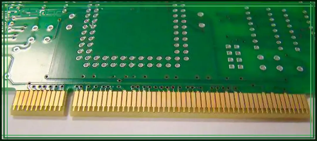
In electronic products such as computer motherboards, graphics cards, servers, SSDs, and industrial control equipment, we often see an interface with gold fingers, which is the PCB edge connector. It achieves electrical connection by inserting a row of gold-plated contacts along the edge of the PCB into the corresponding slot, without the need for additional cables or plastic connector housings.
This connection method is widely adopted mainly due to the following advantages:
• Simple structure and low manufacturing cost
• Compact size, making it suitable for high-density PCB designs
• Stable signal transmission, ideal for high-speed and high-frequency electronic applications
• With hard gold plating, it can withstand hundreds to thousands of mating cycles without performance degradation
In actual design, if the circuit board needs to be connected to the motherboard, expansion card or storage module (such as PCIe slots, DDR memory, GPU or M.2 SSD), it is particularly important to understand the design specification of the PCB edge connector. This includes key contents such as bevelling, surface finishes (ENIG or hard gold), inner copper clearance, dimensional control and IPC industry standards.
This article will systematically introduce the board edge connector from aspects such as principle, type classification, design key points, manufacturing process and application scenarios, to help you reduce mistakes and improve reliability and manufacturability in the PCB design and production process.

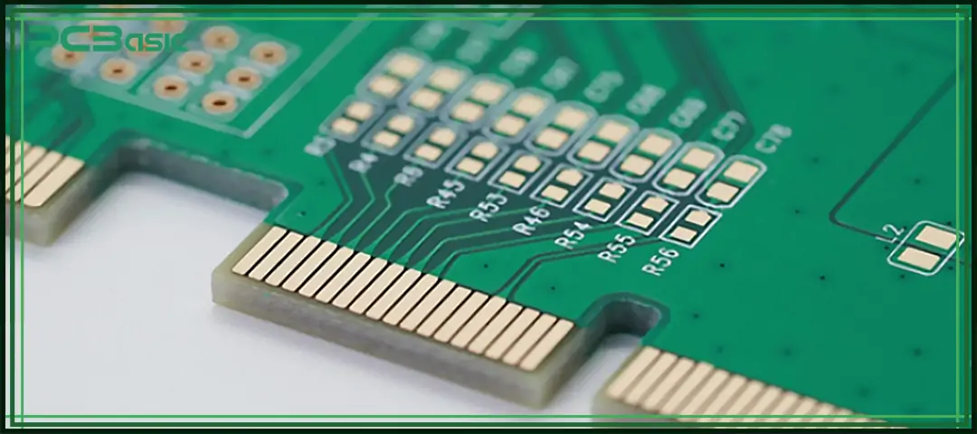
A PCB edge connector, simply put, is a row of conductive pads placed along the edge of a PCB and connects circuits by inserting them into slots. This design is commonly known as "gold fingers". Once inserted into the motherboard or expansion slot, electrical signals can be transmitted between the two devices.
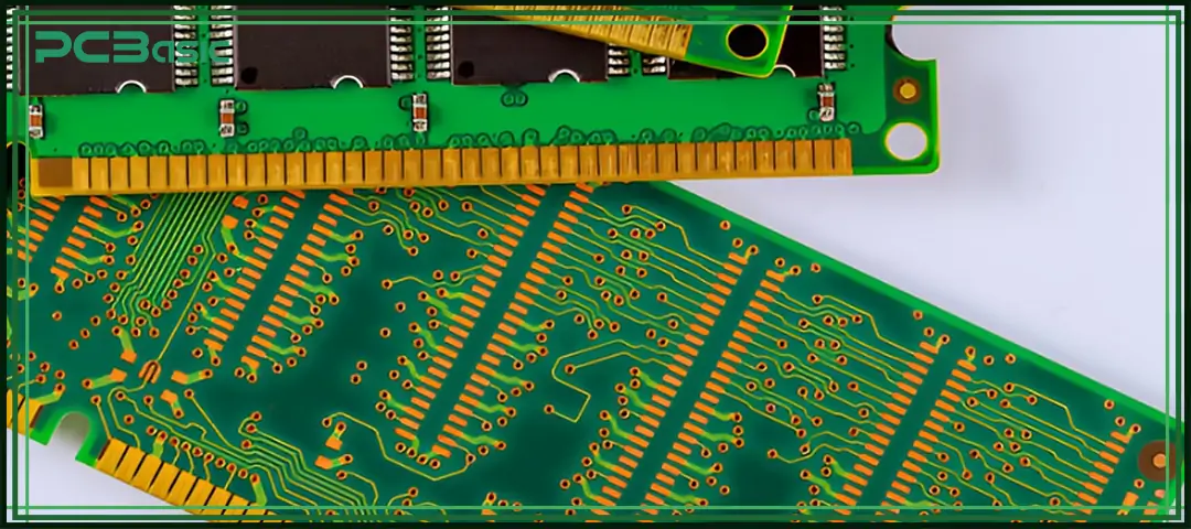
The surface of these gold fingers is usually nickel-plated first and then hard gold plated. This can prevent wear and ensure reliable contact even when they are repeatedly inserted and removed. This kind of PCB edge connector can be seen on things like graphics cards, memory modules (DDR), PCIe expansion cards, backplanes of communication equipment, and SSD storage devices.
The characteristics of the PCB edge connector are very distinct. Firstly, its pads are directly designed on the edge of the PCB board to be inserted into the slots for connection, eliminating the need for additional plastic connector housings. Therefore, the structure is simpler and occupies less space.
Secondly, the board edge connector can stably transmit high-speed and high-frequency signals, making it highly suitable for electronic devices such as computer motherboards, graphics cards, servers, and SSDs that have high requirements for signal integrity.
To ensure reliability, the PCB edge connector takes into account the insertion and extraction life during design. Generally, it can withstand more than 500 to 1,000 cycles without affecting performance. If a hard gold coating is adopted, the frequency can be even higher. Therefore, it not only saves costs and space, but also has durability and stability.

PCB edge connectors are not a single fixed structure but are classified differently based on design methods and application scenarios. There are two common classification methods: one is based on the design structure of the solder pads, such as regular gold fingers, segmented gold fingers, and long-short gold fingers. Another type is classified by application standards, such as edge card, compactPCI, PCIe, memory interface, etc. Understanding these types can help us choose the most suitable connection method when designing.
|
Connector Type |
Description |
Typical Use |
|
Regular Gold Fingers |
Equal pad length and spacing |
PCIe GPU, network cards |
|
Segmented Gold Fingers |
Pads divided by insulating slots |
Special isolated signals |
|
Long and Short Fingers |
Pads have different lengths to control power or signal sequencing |
USB drives, SD cards |
Edge Card Connectors
This is the most basic and common type of PCB connectors. The structure is simple--just insert the PCB with gold fingers into the slot, and the connection is complete. It is often used in some low-speed or cost-sensitive electronic devices.
CompactPCI
This kind of PCB edge connector is mainly used in industrial equipment. It usually has multiple rows of contacts, high mechanical strength, and is not easy to loosen; it can withstand harsh environments such as vibration and shock. This PCB edge connector is very suitable for industrial control systems and communication equipment.
PCI Express(PCIe)
It is the most common high-speed edge connector standard in modern computers. It is used to connect high-bandwidth devices such as graphics cards (GPUs), solid-state drives (SSDs), and AI accelerator cards, featuring fast transmission speed and high stability.
Memory Edge Connectors
These PCB edge connectors are specifically designed for memory and storage devices, such as DDR3/DDR4/DDR5 RAM modules, laptop memory, M.2 NVMe SSDS, etc. These can complete an electrical connection after being inserted into the motherboard without the need for additional cables.
The contact area of the PCB edge connector is inserted and removed repeatedly. If the surface plating is poor, it is very likely to wear out, oxidize or cause unreliable electrical contact. So, in the gold finger area, choosing the appropriate surface finish is very crucial, as it will directly affect the conductivity, durability and service life of the edge connector. The two most common surface finishes are ENIG (Electroless Nickel Immersion Gold) and Hard Gold (electroplated hard gold).
|
Surface Finish |
Thickness |
Usage |
Properties |
|
ENIG (Electroless Nickel Immersion Gold) |
1–3 μ |
Prototyping, low mating cycles |
Soft, solderable, flat surface |
|
Hard Gold (Electroplated) |
20–50 μ |
High-durability PCB edge connectors |
Wear-resistant, corrosion-proof |
Most PCB edge connectors are electroplated with hard gold because it can withstand more than 1000 mating cycles. Under the gold layer, a nickel layer of approximately 3 - 7 μm is electroplated first to enhance adhesion and prevent oxidation.

In order to make the board edge connector insert more smoothly, the edge of the PCB needs to be beveled, that is, chamfered. This can prevent the gold fingers from being scratched during insertion and removal, and also make it easier for the insertion position to align with the slot.
Common chamfer specifications include:
• Standard bevel angle: 30°
• Special options: 20°, 45°, 60°
• Minimum remaining material after bevel: 0.25 mm
• PCB thicknesses commonly used: 1.6 mm, 2.0 mm, 2.4 mm
• PCBs smaller than 50 mm × 50 mm may not support proper chamfering
Chamfering is usually carried out after the gold plating or surface treatment of the PCB edge connectors is completed. If the chamfer angle is incorrect, the edge is too sharp, or the processing is rough, it may scratch the slot and even affect the contact effect.

Time is money in your projects – and PCBasic gets it. PCBasic is a PCB assembly company that delivers fast, flawless results every time. Our comprehensive PCB assembly services include expert engineering support at every step, ensuring top quality in every board. As a leading PCB assembly manufacturer, we provide a one-stop solution that streamlines your supply chain. Partner with our advanced PCB prototype factory for quick turnarounds and superior results you can trust.
Designing a reliable PCB edge connector requires following a series of manufacturability rules to avoid electrical faults, exposed copper or pad damage. These design guidelines ensure that the edge connector can be precisely inserted into the slot and can withstand repeated insertions and removals.
To prevent short circuits or exposed copper after bevelling:
|
Design Requirement |
Minimum Value |
|
Pad/Via distance to edge connector area |
≥ 2.0 mm |
|
Edge of PCB to start of PCB edge connector pad |
≥ 0.5 mm |
|
Inner layer copper clearance at 30° bevel |
≥ 2.0 mm |
|
Inner layer copper at 45°/60° bevel |
≥ 1.0 mm |
|
Maximum single pad length |
≤ 40 mm |
If the inner copper foil is too close to the board edge connector, copper may be exposed during chamfering processing, causing short circuits or corrosion.
In the PCB edge connector (gold finger) area, the solder mask layer cannot be covered. The gold finger pads must be kept completely exposed to ensure stable contact with the slot. If the solder mask ink covers the pads, it will affect the conductivity and insertion and extraction performance.
Similarly, silkscreen elements such as reference designators, text labels, and polarity marks cannot be printed on the edge connector pads either, to avoid contaminating the contact surface or affecting the gold plating quality.
In addition, when designing the board edge connector, the inner copper foil also needs to avoid the chamfer area to prevent copper exposure during the cutting process. There are two common copper removal methods:
• Half-finger removal: only remove the inner layer of copper directly beneath the gold finger pad.
• Full-finger removal: completely remove copper from all layers of the entire gold finger area to ensure that no inner layer metal is exposed after chamfering.
When designing the PCB edge connector, it must be placed on the straight edge outside the PCB to allow proper machining and insertion. If there are edge connectors on both sides, a distance of at least 150mm should be maintained between them.
When producing spliced boards, chamfering must be carried out after the boards are separated and cannot be processed in advance. In addition, the size of the PCB in the direction perpendicular to the connector should be controlled within 40 to 400 mm, so as to be compatible with standard chamfering equipment.

To ensure that PCB edge connectors have good durability and performance, manufacturers usually follow industry standards such as IPC-6012 and IPC-A-600.
Solder Mask Application
Mask applied over copper except in the edge connector area.
Nickel Plating
3–7 μm thick nickel underlayer ensures hardness and corrosion resistance.
Hard Gold Plating
20–50 μ” thick surface applied on the edge connectors.
Bevelling / Chamfering
Done at 20°, 30°, 45°, or 60° after plating.
Cleaning and Inspection
Remove residue and inspect finish.
|
Test |
Purpose |
|
AOI (Automated Optical Inspection) |
Detect surface defects, mask issues |
|
Tape Adhesion Test |
Ensures gold plating strongly adheres to nickel and substrate |
|
X-Ray (optional) |
Examines inner copper clearance during beveling |
|
Thickness Measurement |
Confirms ENIG or hard gold meets the required μ" level |
Gold used on a PCB edge connector typically includes 3–15% cobalt to increase hardness and reduce surface wear.
PCB edge connectors are used in several industries and products:
|
Industry |
Application Example using edge connector |
|
Computers & Servers |
PCIe graphics cards, RAM modules, M.2 SSDs |
|
Telecommunications |
CompactPCI systems, network cards |
|
Consumer Electronics |
SD cards, USB devices, TV tuner cards |
|
Industrial Automation |
Control modules, PLCs, data acquisition cards |
|
Automotive & Aerospace |
Embedded computing modules, diagnostic boards |
The reason why PCB edge connectors have been widely used is that it is simple, durable, low-cost, and can stably achieve the connection between boards. Whether it's a high-speed PCIe interface or a common memory card slot, edge connectors can offer reliable electrical conductivity, take up little space, and have a robust structure.
In order to make the PCB edge connectors last longer and be more stable, the correct types of PCB connectors must be selected during the design. At the same time, pay attention to whether the surface finishes (such as ENIG or hard gold) and chamfering treatment are correct, and whether they comply with the IPC manufacturing standards. As long as these details are well handled, the board edge connectors produced can withstand repeated insertions and removals, and their performance will not decline.

Assembly Enquiry
Instant Quote
Phone contact

+86-755-27218592
In addition, we've prepared a Help Center. We recommend checking it before reaching out, as your question and its answer may already be clearly explained there.
Wechat Support

In addition, we've prepared a Help Center. We recommend checking it before reaching out, as your question and its answer may already be clearly explained there.
WhatsApp Support

In addition, we've prepared a Help Center. We recommend checking it before reaching out, as your question and its answer may already be clearly explained there.