Global high-mix volume high-speed PCBA manufacturer
9:00 -18:00, Mon. - Fri. (GMT+8)
9:00 -12:00, Sat. (GMT+8)
(Except Chinese public holidays)
Global high-mix volume high-speed PCBA manufacturer
9:00 -18:00, Mon. - Fri. (GMT+8)
9:00 -12:00, Sat. (GMT+8)
(Except Chinese public holidays)
HomePage > Blog > Knowledge Base > RF PCB Design Guidelines
High-frequency electronics technology has become the core of modern wireless communication, Internet of Things (IoT) and sensor applications. Therefore, it is very important for engineers to master RF PCB design. Unlike ordinary PCBs, radio frequency printed circuit boards (RF PCBs) are strongly affected by parasitic effects, material properties and electromagnetic interference during operation.
Many engineers think that RF PCB design and layout are like "black magic", but in fact, they are not. Efficient RF PCB design relies on physics and clear planning, such as choosing appropriate RF board materials, designing reasonable stacking structures, and precisely arranging the positions of components.
In this guide, it will provide you with a complete RF PCB design roadmap, gradually unfolding from industry experience, practical skills to common RF PCB design guidelines. You will learn the key points from substrate selection to advanced RF PCB layout, and fully master how to design high-performance RF PCBs to meet today's demands for high speed, stability and efficiency.
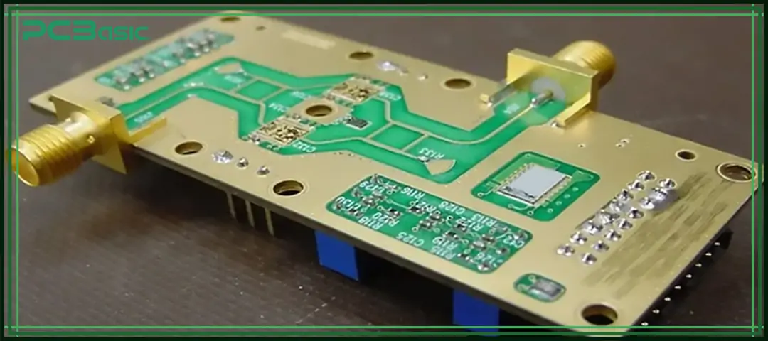
First, let's understand a question: what is an RF PCB?
An RF PCB (Radio Frequency Printed Circuit Board) is a circuit board specifically used for processing high-frequency signals. In the PCB industry, boards operating frequencies exceeding 100 MHz are usually called radio frequency PCBs, while designs with frequencies exceeding 2 GHz are classified as RF microwave PCBs.
Unlike ordinary PCBs, RF boards are affected by parasitic capacitance, parasitic inductance, dielectric losses and radiation. If not handled properly, these factors will greatly reduce the performance of the circuit. Therefore, RF PCB design is more complex than ordinary PCBs, requiring precise control of impedance, ground and signal traces. Even a small trace width, bend radius or via placement may affect the effect of RF layout.
RF circuit boards have a wide range of applications, including:
• Wireless communication systems, including Wi-Fi, Bluetooth, and 5G
• IoT devices and RF sensors
• Smartphones and consumer electronics
• Automotive radar and advanced driver-assistance systems
• Robotics, aerospace, and defense systems
• High-speed mixed-signal electronics
The goal of RF PCB design is to combine principles of RF design with precise RF layout technology to ensure clean signals, reduce electromagnetic interference (EMI), and maintain stability at high frequencies. Whether it is designing compact RF boards for consumer products or developing multilayer RF microwave PCBs for critical tasks, the goal is the same: make RF circuit boards that can reliably transmit and process high-frequency signals.
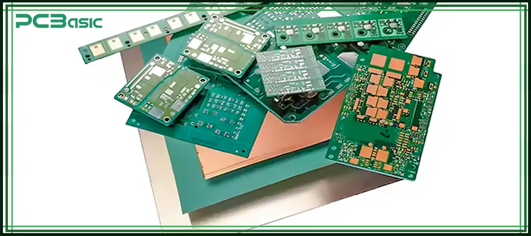
In RF PCB design, choosing the appropriate substrate material is significant. The dielectric properties, thermal performance, and mechanical stability of the substrate will directly affect the performance of the RF PCB design.
The main factors to be considered include:
• Dielectric constant (εr): Determines the propagation speed and impedance of the signal. The more uniform εr is, the more stable the performance of the RF PCB will be.
• Loss tangent: Represents the proportion of signal energy lost as heat. Low-loss materials can reduce the signal attenuation in RF circuit boards.
• Thermal expansion (CTE): Ensures the dimensional stability of the board when the temperature changes, without affecting its performance.
Commonly used RF PCB materials include:
• FR-4: It is cost-effective but has a significant loss at very high frequencies
• Rogers RO3000 and RO4000 series: Low-loss, suitable for RF microwave PCBs
• Teflon-based substrates: Excellent performance, suitable for advanced RF boards
Choosing the appropriate substrate enables engineers to strike a balance among performance, cost and manufacturability, while meeting the requirements of the RF PCB design guidelines.
A good RF layout should start with a reasonable stacking structure. The stacked structure not only affects impedance control but also reduces the interference of RF PCBs.
The following is a suggested table for RF PCB layer stack-up and grounding guidelines:
|
Category |
Recommendation/Method |
Purpose/Explanation |
|
Layer Stack-Up |
Place RF traces on the top layer |
Minimize parasitic coupling and improve signal integrity |
|
Ground planes immediately below RF traces |
Provide a return path and reduce EMI |
|
|
Separate analog, digital, and RF PCBs |
Prevent cross-coupling and interference between signals |
|
|
Grounding |
Maintain continuous ground planes under RF traces |
Ensure stable impedance and provide a low-resistance return path |
|
Use via stitching or via fences |
Connect the top and bottom ground layers to strengthen grounding |
|
|
Avoid placing signal layers between bias and ground layers |
Minimize noise coupling and maintain clean signals |
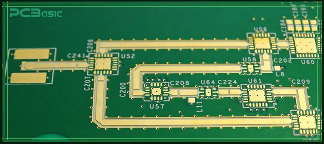
In RF PCB design, the transmission of high-frequency signals is different from that of low-frequency signals, so the design of traces is very crucial. A good RF board design can ensure stable impedance, reduce signal reflection, and maintain signal integrity.
Common types of transmission lines include:
|
Transmission Line Type |
Description |
Application |
|
Microstrip |
Conductor trace over a solid ground plane, easy to implement |
Widely used in RF PCBs |
|
Stripline |
Embedded between two ground planes, provides excellent isolation |
Suitable for RF microwave design |
|
Suspended Stripline |
Center conductor with ground planes above and below |
Used for precise RF PCB design |
|
Coplanar Waveguide (Grounded) |
Center trace flanked by ground planes |
Ideal for RF boards requiring high isolation |
When designing traces, it should be noted that the impedance should be controlled at 50Ω or 75Ω, which is very important for RF circuit boards. For curved traces, the bend radius should be at least three times the trace width to maintain impedance stability. If a right-angle bend must be used, angled miter compensation (Douville & James formula) should be applied to reduce impedance discontinuities.
In RF PCB design, the choice between curved and mitered bends depends on the frequency and space. RF boards above 10 GHz are more suitable for using curved traces, while for low-frequency applications, mitered bends can be adopted.
Time is money in your projects – and PCBasic gets it. PCBasic is a PCB assembly company that delivers fast, flawless results every time. Our comprehensive PCB assembly services include expert engineering support at every step, ensuring top quality in every board. As a leading PCB assembly manufacturer, we provide a one-stop solution that streamlines your supply chain. Partner with our advanced PCB prototype factory for quick turnarounds and superior results you can trust.
In RF PCB design, we should not only pay attention to the traces, but also to the component placement, which is crucial. Reasonable component arrangement can reduce parasitic effects, improve signal stability, and make RF circuit boards easier to manufacture at the same time.
In practice, RF components should be placed as close as possible to shorten the length of the traces. Digital, analog and radio frequency modules should be placed separately to avoid mutual interference. Give priority to using surface-mount components to make the layout of the RF PCB more compact. Adding shielding, such as golden rings and via fences, can reduce electromagnetic interference (EMI). Meanwhile, attention should also be paid to thermal management. The ground plane and via array help the RF boards dissipate heat.
Arranging components in accordance with the RF PCB design guidelines is the key to ensuring stable high-frequency performance and reducing unnecessary radiation.
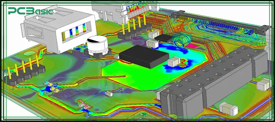
Before manufacturing, the RF PCB design must be verified through advanced simulation tools. RF PCBs are highly sensitive to subtle layout changes, so simulation is of vital importance.
|
Item |
Description |
Example Tools/Methods |
|
EM Simulation |
Analyze the electromagnetic behavior of RF PCBs to ensure signal integrity and EMI control |
ANSYS SIwave, Cadence Microwave Office, Allegro X PCB Designer |
|
S-Parameter Extraction |
Analyze insertion loss, return loss, and impedance matching |
Dedicated S-parameter simulation modules |
|
Frequency-Domain Simulation |
Evaluate RF microwave design performance across different operating bands |
Built-in frequency-domain analysis features in simulation software |
|
Design Automation |
Quickly test variations in trace width, bend radius, and component placement to optimize performance |
Design automation modules in Cadence PCB tools |
Modern RF PCB design leverages sophisticated CAD tools and advanced layout strategies to achieve high-performance RF microwave PCBs.
Tips for Optimal RF Design:
• Prefer curved bends over mitered bends at high frequencies (>10 GHz).
• Use via fences and stitching to isolate critical RF traces.
• Minimize parallel routing of high-speed digital and RF signals.
• Implement shielding and grounded pads for sensitive components.
• Carefully design layer stack-up with proper bias and ground separation.
• Optimize decoupling capacitors and use multiple SRF ranges.
• Apply 3D EM field solvers to validate designs for signal integrity and loss.
By following these RF PCB design guidelines, engineers can design RF boards with excellent performance, strong manufacturability and reliability.
Designing a radio frequency PCB involves multiple aspects and requires a clear understanding of RF design, material selection, stacking structure, transmission lines, component layout, power routing and simulation. Modern RF microwave design tools can assist engineers in creating high-performance RF boards, ensuring precise impedance, reducing electromagnetic interference (EMI), and stable operation at different frequencies.
Whether you are taking the RF PCB design course, making RF circuit boards for wireless applications, or developing multilayer RF microwave PCBs, following these best practices can all make your RF PCB design more reliable. Through simulation, reasonable stacking design, component layout and shielding methods, engineers can produce high-quality RF PCBs that can be put into production.
With the increasing demand for wireless devices, IoT sensors, and radio frequency PCBs, mastering the skills of RF PCB design and RF layout has become extremely necessary.

Assembly Enquiry
Instant Quote
Phone contact

+86-755-27218592
In addition, we've prepared a Help Center. We recommend checking it before reaching out, as your question and its answer may already be clearly explained there.
Wechat Support

In addition, we've prepared a Help Center. We recommend checking it before reaching out, as your question and its answer may already be clearly explained there.
WhatsApp Support

In addition, we've prepared a Help Center. We recommend checking it before reaching out, as your question and its answer may already be clearly explained there.