Global high-mix volume high-speed PCBA manufacturer
9:00 -18:00, Mon. - Fri. (GMT+8)
9:00 -12:00, Sat. (GMT+8)
(Except Chinese public holidays)
Global high-mix volume high-speed PCBA manufacturer
9:00 -18:00, Mon. - Fri. (GMT+8)
9:00 -12:00, Sat. (GMT+8)
(Except Chinese public holidays)
HomePage > Blog > Knowledge Base > PCB Design Basics: A Design Guide for Beginners
Circuit boards are everywhere, and they form the foundation of all the electronic products we use. To make these circuit boards truly functional, proper PCB design is indispensable. Good PCB design ensures the intended functionality of the device. Essentially, printed circuit board design is the process of converting schematic diagrams into manufacturable layouts. During this process, we must clearly understand the fundamentals of PCB design, because only in this way can the designed circuit boards help the equipment achieve the expected functions and operate stably for a long time. However, designing PCBs is not just about drawing a few lines with software.
Next, this article is here to help you master the basics of PCB design. In this article, we will guide you through PCB design with clear and practical steps. After reading this article, you will learn how to plan projects, draw schematics, and place components reasonably. Below are the basic knowledge points related to PCB design that we have summarized.
|
Stage |
Goal |
Beginner Key Points (Actionable) |
Common Mistakes |
Quick Check / Metrics |
|
Planning |
Define functions, constraints, cost |
List functions & I/O; define board outline & mounting holes; estimate power; lock key IC packages; draw block diagram |
Start layout without size/power limits; ignore heat/power |
Deliverables: spec sheet + BOM v0 + block diagram |
|
Library |
Correct symbols/footprints |
Map each symbol to the right footprint; define Pin1/polarity; use consistent naming |
Symbol-footprint mismatch; missing pad attributes |
Randomly preview 10% of footprints |
|
Schematic (SCH) |
Accurate, readable, testable |
Modular drawing; add decoupling caps for every VCC; add test pads/debug ports; clear net labels |
Hidden power pins wrongly connected; wrong polarity/direction |
ERC all green; critical nets explicitly named |
|
BOM & Sourcing |
Components available & replaceable |
Choose common packages; assign A/B alternates for key parts; mark lifecycle |
Exotic packages; no alternatives |
Alternate PN listed; lead time >8w flagged |
|
Stack-up |
Continuous reference planes, easy routing |
2L: bottom as ground; 4L: signal/ground/power/signal; confirm dielectric/impedance with fab |
Split planes; signals crossing splits |
High-speed nets have continuous ground; impedance layer pair |
|
Placement |
Short loops, low coupling, good assembly |
Place power near load; crystal close to IC; diff pairs near connector; I/O on edges; decoupling next to pins |
Far decoupling; ignore height/clearance |
3D fit check; copper/airflow near hot parts |
|
Routing |
Manufacturable, low-noise |
Route power & ground first, then high-speed, then analog, then low-speed; 45° corners; few vias; stitch ground vias |
90° corners; via clusters; crossing splits |
Wide power traces; diff pairs matched; ≤2 layer swaps on critical nets |
|
High-speed/Differential |
Timing & integrity |
Pair tightly, equal length, reference plane continuous; follow termination guide |
Crossing gaps; skew too large |
Clock/diff skew < spec; no plane splits |
|
PDN/Power |
Low impedance, stable rails |
Multi-frequency decoupling (0.1µF + 1µF + 10µF); short loops; multi-via for high current |
Rely on one big capacitor; large loops |
Short/local decoupling loops visible |
|
Vias |
Reliable, manufacturable |
Correct drill/annular ring; multi-via for current; via-in-pad only if controlled |
Too small annular rings; open via-in-pad |
Min drill/ring meets fab rules; thermal relief OK |
|
Silkscreen/Polarity |
Easy assembly & debug |
Clear refs; Pin1/polarity marks; no pads covered; arrows for orientation |
Silkscreen on mask; unclear polarity |
Check diodes/e-caps/IC orientation |
|
Design Review |
Systematic verification |
Run DRC/ERC; continuity check; 3D enclosure fit; test access; consistent net names |
Only DRC, no manual check |
DRC all green + manual checklist |
|
Manufacturing Files |
Complete, unambiguous |
Gerber/Drill; BOM; PNP file; assembly drawing; fab notes (thickness/copper/finish/impedance) |
Missing/mirrored layers; silkscreen on pads; bad filenames |
Cross-check in Gerber viewer |
|
Proto → Mass Production |
Risk control |
Prototype first; include test pads; FCT/scan ready; review before MP |
Skip proto; no test strategy |
Proto passes FCT & thermal tests |
|
Topic |
Goal |
Beginner Key Points |
Common Mistakes |
Quick Check / Metrics |
|
Signal Integrity (SI) |
Reduce reflection/crosstalk |
Controlled-impedance traces over solid ground; diff pairs equal length; space parallel sensitive lines |
Crossing splits; long parallel runs |
Length/spacing/stack-up per spec |
|
Power Integrity (PI/PDN) |
Low impedance rails |
Multi-frequency decoupling; copper pours/vias for current |
Only one bulk cap; long loops |
Ripple within spec; decoupling close to pin |
|
Grounding |
Continuous, low-noise |
Solid planes; analog/digital zones tied at one point |
Random cuts; large loops |
No high-speed crossing ground gaps |
|
EMI/EMC |
Low radiation, high immunity |
Small loops; CM chokes; filters at connectors |
Signals long to connector |
Filters/shields at I/O |
|
Clock/Crystal |
Low jitter, low noise |
Crystal close to IC; short traces; ground guard; away from I/O edge |
Cross split; long traces |
≤ few mm loop; continuous ground |
|
ESD/Surge |
Protect I/O |
TVS/clamps near port; short path to ground |
Far protection parts |
Direct, short discharge to GND |
|
Creepage/Clearance |
Safe insulation |
Follow safety standards for spacing; use slots if needed |
Guessing instead of spec |
Meets IEC/UL clearance rules |
|
Thermal |
Manage temperature |
Copper pours under hot parts; thermal vias; airflow & heatsinks |
Hotspots |
ΔT < component rating |
|
Mechanical/Assembly |
Fit, serviceability |
3D enclosure fit; connector alignment; height check |
Ignore height/fit |
No 3D interference; connectors aligned |
|
DFM (Fabrication) |
Manufacturable |
Line/space/drill ≥ fab limits; solder mask bridge ≥ min; copper edge ≥0.3mm |
Over-spec design |
Matches fab capability |
|
DFA (Assembly) |
Easy solder/placement |
Same orientation; spacing; thermal relief pads; stencil matched |
Silkscreen on pads; tombstoning |
First article solder OK |
|
DFT (Testability) |
Test-ready |
Add test pads; JTAG/SWD/UART; FCT fixture ready |
No test access |
ICT/FCT coverage ≥ goal |
|
Panelization/Fixtures |
Efficient build |
Panel rules; fiducials; tooling holes; strong rails |
Random break-tabs |
Panel accepted by Fab |
|
Docs/Versioning |
Traceable |
Version/rev; BOM matches PNP; fixed export settings |
Confused docs |
Doc pack complete & consistent |
|
Compliance/Green |
Legal & safe |
Mark RoHS/REACH; plan EMC countermeasures; shield key ports |
No proof |
Certificates in place |
|
Reliability/Derating |
Long life |
Derate stress; connector cycles; conformal coating |
Zero margin |
Parts at ≤70–80% rating |
Next, let's directly start designing the PCB.

Planning is an indispensable step before starting PCB design and is a core step in circuit board design. The purpose of planning is to first clearly define the functional goals of the circuit board, such as which inputs and outputs are needed; at the same time, assess its working environment, including power supply voltage and current, operating temperature range, and other usage conditions. In addition, cost and development cycle also need to be considered, such as the number of layers of the circuit board and the time required for prototyping and material preparation.
After these key points are confirmed, one can start preparing the first version of the Bill of Materials and conduct cost and manufacturability analysis. After completing the above planning, we usually obtain: complete requirements and specifications, block diagrams between functional modules, and BOM v0 with packaging and alternative material information.
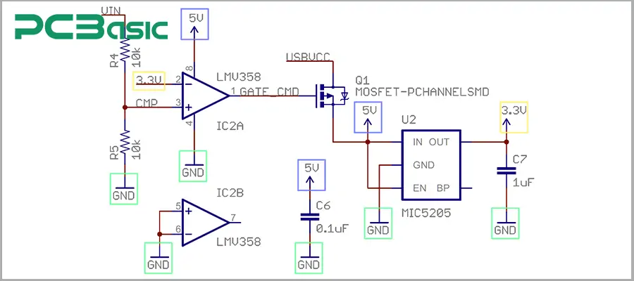
The schematic diagram is like the "map" of a circuit. First, we need to select the appropriate EDA tools, and establish the project structure. Then, we need to prepare and verify the component library to ensure that the symbols and footprints are one-to-one correspondence. Next, for each IC, we need to add the necessary peripheral circuits, such as decoupling capacitors, reset circuits, crystal matching networks, and pull-up and pull-down resistors. At the same time, we also need to reserve test points and debugging interfaces.
During the verification stage, we should use the ERC tool to confirm whether the power pins are connected correctly, whether the interface polarity is correct, whether the differential pairs are not swapped, and whether the reference design values are reasonable. Only in this way can we obtain a clean schematic diagram and the initial BOM that pass the ERC check.
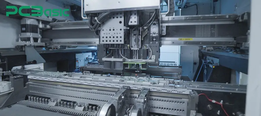
The component layout determines the signal flow, heat dissipation and assemblability of the circuit board. During the layout process, we should follow the modular principle and group related components, such as the power area, analog area, digital area and high-speed interface area. The signal flow is also best to "flow downstream", from input to output, minimizing the circuit area as much as possible.
We also need to give priority to the placement of key components. For example, the power chip should be close to the load and current loop, and decoupling capacitors must be close to the power pins, etc. During the layout, we should also avoid screw holes and snap-in areas to maintain a reasonable copper sheet to board edge distance.
To facilitate detection and assembly, similar components should be uniformly oriented, leaving safe space for welding and pick-and-place nozzles. This can avoid common errors such as too far distance between the power supply and high-speed components, too far placement of decoupling capacitors, or interference of component height with the enclosure.
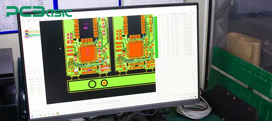
After the layout is completed, it enters the PCB layout stage, which includes board frame, layer stacking, and rule settings, etc. First, we need to define the shape of the board, chamfering, slotting, and whether V-CUT or paneling is required. Then, we set the Keepout area. Electromagnetic and thermal design are equally crucial. We should prioritize planning the ground reference plane to provide the shortest path for return current, and at the same time, lay copper under the heat-generating components and drill thermal through-holes. Finally, don't forget to reserve positioning reference points, tool holes, and test points. These basic settings will directly determine the difficulty of subsequent routing and the performance of the finished product.
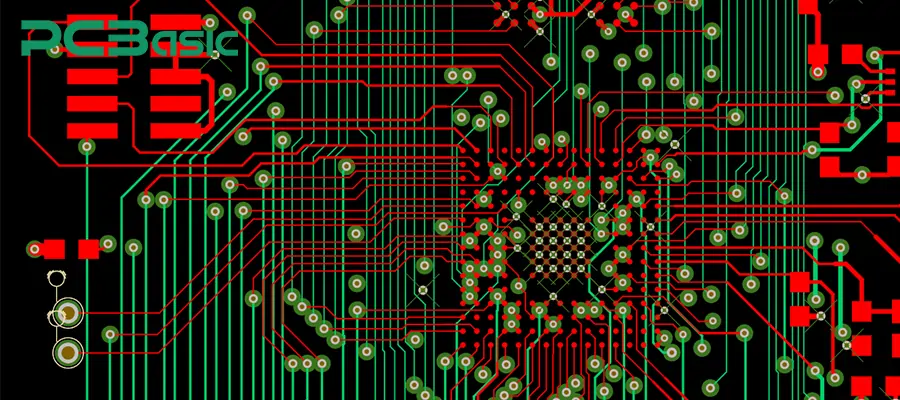
Routing is the process of physically connecting components to form a circuit. The sequence of routing has priorities: first are high-current power supplies and grounds, followed by high-speed, clocks, and differential signals, then analog-sensitive signals, and finally low-speed general-purpose I/O.
The basic techniques for routing include:
Try to keep the lines short and straight, and minimize the use of 90-degree corners.
When changing layers, try to place the grounding vias close to the layer change to ensure a continuous return path.
Maximize the width of the power and ground traces or use a full sheet of copper.
For high-speed differential traces, maintain equal length, equal spacing, and the same reference plane.
Avoid crossing through partition surfaces and perform terminal matching at the endpoints.
Separate analog and digital signals to avoid mutual interference.
Common mistakes in wiring include interruption of ground reference, long loops, trace width, or excessively long power return paths. Mastering these wiring techniques is very helpful for improving the quality of circuit board design.
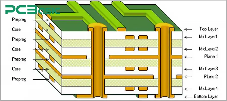
The number of layers and stack structure of a PCB determine its wiring capability and signal integrity. A single-layer board has the lowest cost and is best suited for simple circuits and educational purposes; a double-layer board is the preferred choice for entry-level designs. Multi-layer boards with four or more layers are widely used in high-speed and complex products such as mobile phones and servers.
If you are designing for high-speed or RF applications, you also need to verify the dielectric constant and stack-up parameters with your PCB manufacturer. Moreover, please note that a continuous ground layer should be maintained below high-speed signals, and use stitching vias in key areas. This reasonable layering design can reduce noise and significantly simplify wiring.
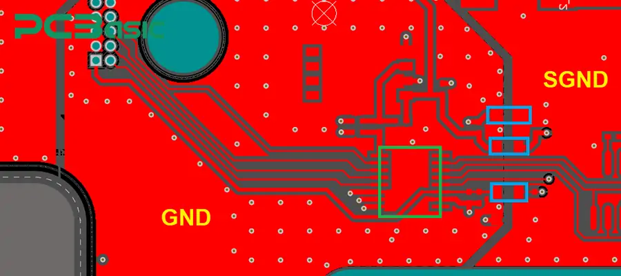
The power supply and ground plane form the foundation for the stable operation of the circuit. In terms of grounding strategy, it is preferable to ground the entire surface uniformly without making arbitrary divisions. For large current circuits, the area should be minimized and closely attached to the wiring to reduce electromagnetic radiation. Regarding power supply strategy, it requires the placement of decoupling capacitors near the IC power pins, using a combination of small and large capacitors, and keeping the circuit as short as possible.
Sensitive analog and digital power supplies can be isolated using magnetic beads or LC circuits before being merged into the main power supply. For high-current rails, wider traces or dedicated power planes should be used, and current is dissipated through multiple vias. Large copper sheets require "thermal pads" for easy soldering, and sufficient vias should be placed on the power and ground planes. Mastering these techniques is also very helpful for circuit board design.
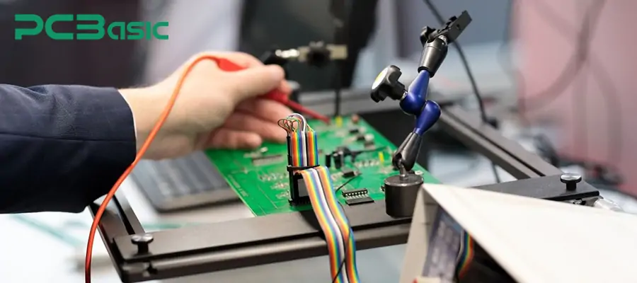
Before conducting PCB manufacturing, it is recommended to conduct a systematic inspection, which can significantly reduce rework. The inspection includes DRC and ERC checks.
DRC focuses on whether the line width/spacing, vias/pads, copper-to-board edge distance, solder mask bridges, etc. comply with the manufacturer's capabilities; ERC confirms whether the power network, unconnected pins, interface polarity and network naming are reasonable. Manufacturing and assembly checks are also important, for example, the silkscreen should be clear, not covering the pads, the test points should be sufficient and easy for the probes to contact. It is also necessary to ensure consistency in BOM, packaging, part numbers and placement coordinates, etc. Thoroughly inspecting the PCB design before manufacturing can ensure the smooth production of subsequent PCBs.
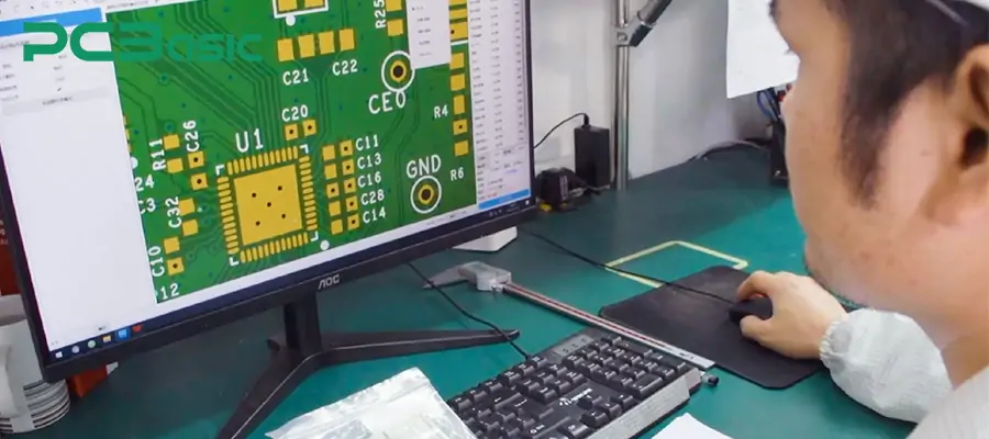
The final step in PCB design is to convert the design into factory-ready materials.
Firstly, we need to export Gerber files, drilling files, as well as assembly information (BOM, Pick-and-Place files, assembly drawings, etc.). If necessary, we also need to provide netlist and board fabrication instructions. During this process, we must clearly indicate the board thickness, copper thickness, layering, surface treatment, solder mask color, and impedance requirements. It is best to carefully review with a Gerber viewer after exporting to avoid errors such as missing layers, mirror images, or solder mask pressing onto the pads.
Note: If you are ordering from a factory for production, it is best to confirm their manufacturing capabilities before placing the order, including the minimum line width/spacing, hole diameter, board thickness, and delivery date. Generally, we should first make a small batch prototype and verify it is error-free before entering mass production.
PCB design is a systematic engineering process that requires planning, verification, and repeated refinement. Each step has a direct impact on the final performance and reliability of the circuit board. For beginners, mastering these basic procedures and key points usually enables them to avoid common design errors.
 About PCBasic
Time is money in your projects – and PCBasic gets it. PCBasic is a PCB assembly company that delivers fast, flawless results every time. Our comprehensive PCB assembly services include expert engineering support at every step, ensuring top quality in every board. As a leading PCB assembly manufacturer, we provide a one-stop solution that streamlines your supply chain. Partner with our advanced PCB prototype factory for quick turnarounds and superior results you can trust.

Assembly Enquiry
Instant Quote
Phone contact

+86-755-27218592
In addition, we've prepared a Help Center. We recommend checking it before reaching out, as your question and its answer may already be clearly explained there.
Wechat Support

In addition, we've prepared a Help Center. We recommend checking it before reaching out, as your question and its answer may already be clearly explained there.
WhatsApp Support

In addition, we've prepared a Help Center. We recommend checking it before reaching out, as your question and its answer may already be clearly explained there.