Global high-mix volume high-speed PCBA manufacturer
9:00 -18:00, Mon. - Fri. (GMT+8)
9:00 -12:00, Sat. (GMT+8)
(Except Chinese public holidays)
Global high-mix volume high-speed PCBA manufacturer
9:00 -18:00, Mon. - Fri. (GMT+8)
9:00 -12:00, Sat. (GMT+8)
(Except Chinese public holidays)
HomePage > Blog > Knowledge Base > J-STD-003 – The Essential Guide to PCB Solderability Testing
In the electronics manufacturing industry, the quality of solder joints directly affects the performance and lifespan of the entire electronic product. If the soldering quality is poor, it may lead to circuit failure, equipment malfunction, increase the cost of rework and maintenance, and in severe cases, even bring safety risks. To avoid these problems, manufacturers must conduct solderability testing on circuit boards. This type of test can detect problems such as poor soldering, insufficient wetting or surface oxidation in advance.
Among numerous standards for PCB solderability, J-STD-003 is the most widely used and important one. It specifically stipulates how to evaluate the solderability of bare printed circuit boards, including common surface finishes methods such as HASL, ENIG, Immersion Silver, OSP, and more. Through the tests of the J-STD-003 standard, engineers can confirm whether these surface finishes can form firm and reliable solder joints in actual production, thereby ensuring that subsequent assembly and the overall machine usage are more stable and reliable.
This article will mainly guide you to have a comprehensive understanding of J-STD-003: what it is, why it is so important in electronic manufacturing, what specific testing methods it has, what common defects it can detect, and the differences between it and J-STD-002.
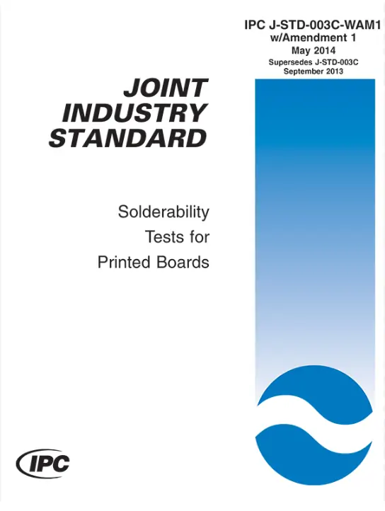
J-STD-003, officially titled Solderability Tests for Printed Boards, is an important industry standard jointly formulated by IPC and JEDEC. It specifies the specific methods and steps for conducting soldering tests on bare PCBs, with the aim of verifying whether the surface treatment layer of the circuit board can be fully wetted with the solder and form a firm bond.
Unlike other standards that focus more on the leads or terminals of electronic components, the test object of J-STD-003 is the circuit board itself before assembly, to ensure that the PCB has good soldering performance before entering the formal assembly process.

Solderability testing not only helps manufacturers identify potential problems with circuit boards during the soldering process, but also eliminates risks in advance before the products officially enter assembly. Only by strictly adhering to J-STD-003 can manufacturers ensure that the surface finish of PCBs has good solderability, providing reliable guarantees for subsequent assembly and the operation of the entire machine.
By following J-STD-003, manufacturers ensure that:
• PCB surface finishes can form strong solder joints.
• Common defects such as non-wetting or dewetting are identified before assembly.
• Long-term product reliability is protected.
• Quality requirements are met for IPC Class 2 and Class 3 products.
The core objective of J-STD-003 is to evaluate the solderability of circuit boards before they enter the assembly process through a series of standardized tests. In actual manufacturing, different PCB surface finish methods will exhibit different characteristics in the J-STD-003 solderability testing. Each process has its own advantages and disadvantages. And potential risks that may arise in the soldering testing.
As these differences will directly affect whether the solder can be evenly wetted and firmly adhered, J-STD-003 provides a unified evaluation framework, enabling engineers to systematically test and verify the reliability of these processes, thereby ensuring that the circuit board has stable and reliable soldering performance in subsequent assembly.
Comparison of PCB Surface Finishes in J-STD-003 Testing
|
Surface Finish |
Characteristics |
Advantages |
Disadvantages |
Key Focus in J-STD-003 Testing |
|
HASL |
Coats copper with molten solder and levels with hot air |
Mature process, low cost, good solderability |
Poor flatness, not suitable for HDI/small pitch |
Check for uneven wetting due to surface roughness |
|
ENIG |
Nickel underlayer with a thin gold coating |
Flat surface, strong oxidation resistance, ideal for BGA/QFN |
Higher cost, risk of “Black Pad” defect |
Verify wetting performance and black pad issues |
|
ENEPIG |
Adds a palladium layer on top of ENIG |
Prevents black pad, excellent compatibility, used in high-end PCBs |
More complex process, higher cost |
Inspect adhesion between multiple metallic layers |
|
Immersion Tin |
Deposits a thin tin layer directly on copper |
Excellent solderability, lead-free compatible |
Poor storage stability, easily oxidized |
Focus on oxidation issues and storage time effects |
|
Immersion Silver |
Deposits a thin silver layer on copper |
Excellent conductivity and solderability |
Sensitive to sulfur and contamination |
Test for cleanliness and anti-tarnish reliability |
|
OSP |
Transparent organic coating protects copper |
Eco-friendly, flat surface, cost-effective |
Short shelf life, moisture-sensitive |
Evaluate film uniformity and effective protection time |

Time is money in your projects – and PCBasic gets it. PCBasic is a PCB assembly company that delivers fast, flawless results every time. Our comprehensive PCB assembly services include expert engineering support at every step, ensuring top quality in every board. As a leading PCB assembly manufacturer, we provide a one-stop solution that streamlines your supply chain. Partner with our advanced PCB prototype factory for quick turnarounds and superior results you can trust.
In J-STD-003 solderability testing, the standard not only stipulates the scope of application but also clarifies several key testing methods. The following introduces three main testing methods:
This is a quantitative solderability testing method that evaluates performance by measuring the wetting force generated when solder comes into contact with PCB pads. During the test, a "force-time" curve will be plotted, from which the speed and degree of solder wetting can be clearly seen. Manufacturers can thereby determine whether different surface treatment processes are easy to form good solder joints. The advantage of this method lies in its ability to provide precise and repeatable scientific data, offering a reliable basis for subsequent process improvements.
This is a more straightforward and easy-to-operate soldering test. During the test, the operator immerses the PCB in the molten solder and then observes the coverage of the solder under magnified conditions. By this method, it is possible to quickly identify whether there are defects such as non-wetting or incomplete coverage. Due to its simple operation and intuitive results, it is often used for rapid monitoring in the production process, helping engineers identify and solve problems in a timely manner.
Different PCB surface finish processes have different performances in solderability, so targeted tests are required. For instance, in the ENIG process, it is necessary to focus on detecting whether there are black pad defects, which are a common risk affecting the reliability of solder joints. OSP coatings, on the other hand, are more susceptible to oxidation, so their antioxidant capacity must be evaluated. J-STD-003 provides a unified evaluation method for these different processes, ensuring that reasonable and reliable test results can be obtained regardless of the surface treatment method adopted.
The core objective of using the J-STD-003 standard is to identify potential issues that may affect solderability through a series of standardized testing methods, thereby ensuring that the circuit board is in the best condition before formal assembly. The common defects mainly include:
• Non-wetting: Solder fails to adhere to certain pads or areas, resulting in missing solder joints, which is usually related to surface contamination or improper surface treatment;
• Dewetting: The solder initially wets the pad, but then retracts or pulls back, leaving the exposed copper surface, which significantly reduces the strength and reliability of the solder joint;
• Voids and incomplete coverage: The solder fails to fully fill or cover the pad area, which can easily cause poor contact or unstable signals;
• Oxidation or contamination: The solder pad or surface finish layer is covered with oxidation, dirt or residual impurities, thereby seriously reducing the wetting performance of the solder.
Through these soldering tests, manufacturers can identify and locate problems at an early stage and take timely repair or process optimization measures, preventing defective circuit boards from flowing into subsequent assembly stages. This not only reduces the high costs brought about by rework and scrapping, but also ensures the stability and reliability of the finished products during their usage.
J-STD-002 is an industry standard that regulates how manufacturers evaluate the solderability of electronic components. Jointly developed by IPC and JEDEC, J-STD-002 provides a unified method to ensure that parts such as terminations, leads, and solder balls can be fully wetted and firmly adhered by solder during PCB assembly. Unlike some general inspection methods, J-STD-002 stipulates strict and detailed procedures. Moreover, J-STD-002 focuses on whether it can be soldered rather than whether the solder joint can work for a long time. Confirming that components have good solderability before entering production helps reduce the defect rate and rework risk, and is one of the most commonly used solderability testing standards.
|
Standard |
Test Object |
Focus |
|
J-STD-002 |
Component terminations (leads, pads, spheres) |
Verifies if components can be reliably soldered; ensures component solderability |
|
J-STD-003 |
PCB surfaces and finishes |
Checks if PCB pads and coatings provide good wetting; ensures PCB solderability |
In simple terms, J-STD-002 focuses on component terminations, while J-STD-003 focuses on PCB surfaces. Only by using the two in combination can the reliability of soldering be fully guaranteed.
In electronic manufacturing, the reliability of solder joints is of vital importance and cannot rely on luck. J-STD-003 provides a set of authoritative industry standards for solderability testing of printed circuit boards, ensuring that different surface finish methods can form strong and durable solder joints. If J-STD-003 is used in combination with J-STD-002, manufacturers can not only verify the solderability of the circuit board, but also ensure the soldering performance of the terminals of electronic components at the same time, thereby improving production yield, reducing soldering defects, and ensuring that the products are safer and more reliable in use.
For PCB manufacturers and assembly factories that pursue high quality, following J-STD-003 is not an option but a fundamental requirement that must be strictly adhered to.

Assembly Enquiry
Instant Quote
Phone contact

+86-755-27218592
In addition, we've prepared a Help Center. We recommend checking it before reaching out, as your question and its answer may already be clearly explained there.
Wechat Support

In addition, we've prepared a Help Center. We recommend checking it before reaching out, as your question and its answer may already be clearly explained there.
WhatsApp Support

In addition, we've prepared a Help Center. We recommend checking it before reaching out, as your question and its answer may already be clearly explained there.